Method and apparatus for calibrating parallel readout paths in imagers

a parallel readout and imager technology, applied in the field of image sensors, can solve the problems of undesirable noise in the readout process, limited operation speed of the above-described readout circuitry, and speed up the circuitry, so as to achieve the effect of reducing the possibility of a boundary

Active Publication Date: 2008-11-18
APTINA IMAGING CORP
View PDF9 Cites 73 Cited by
  • Summary
  • Abstract
  • Description
  • Claims
  • Application Information

AI Technical Summary

Benefits of technology

[0014]Various exemplary embodiments of the invention provide an imaging device with readout chain circuitry that uses multiple analog-to-digital converters and amplifiers, which are similarly calibrated using a stitching technique, to readout each color of a column and mitigate the possibility of a boundary effect.

Problems solved by technology

The operational speed of the above-described readout circuitry is limited by processing constraints particularly as the size of the array 52 increases.
In addition, attempts to speed up the circuitry may introduce undesirable noise into the readout process.

Method used


Image

  • Method and apparatus for calibrating parallel readout paths in imagers
  • Method and apparatus for calibrating parallel readout paths in imagers
  • Method and apparatus for calibrating parallel readout paths in imagers

Examples


Embodiment Construction

[0023]In the following detailed description, reference is made to the accompanying drawings, which form a part hereof and illustrate specific embodiments in which the invention may be practiced. In the drawings, like reference numerals describe substantially similar components throughout the several views. These embodiments are described in sufficient detail to enable those skilled in the art to practice the invention, and it is to be understood that other embodiments may be utilized, and that structural, logical and electrical changes may be made without departing from the spirit and scope of the present invention.

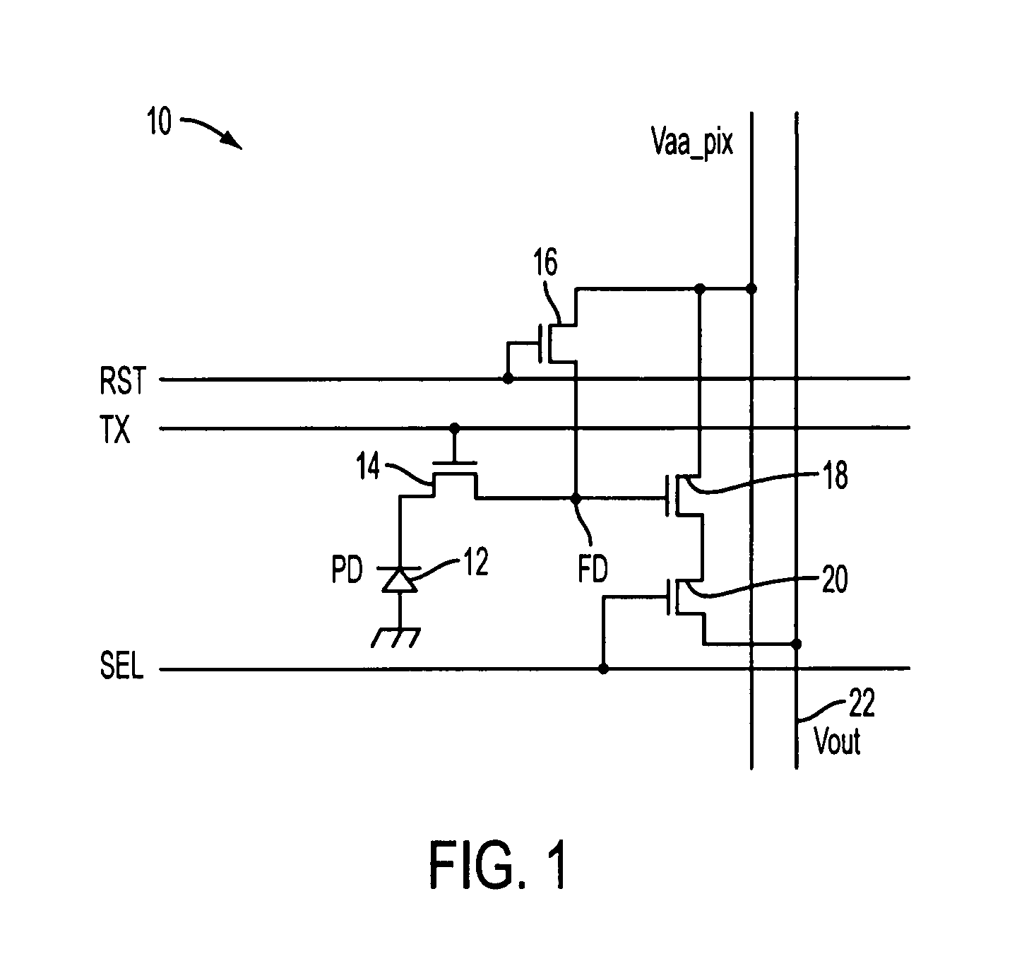
[0024]The term “pixel” refers to a picture element unit cell containing a photo-conversion device and transistors for converting electromagnetic radiation to an electrical signal. It should be appreciated, however, that the invention is not limited to any particular pixel type or configuration.

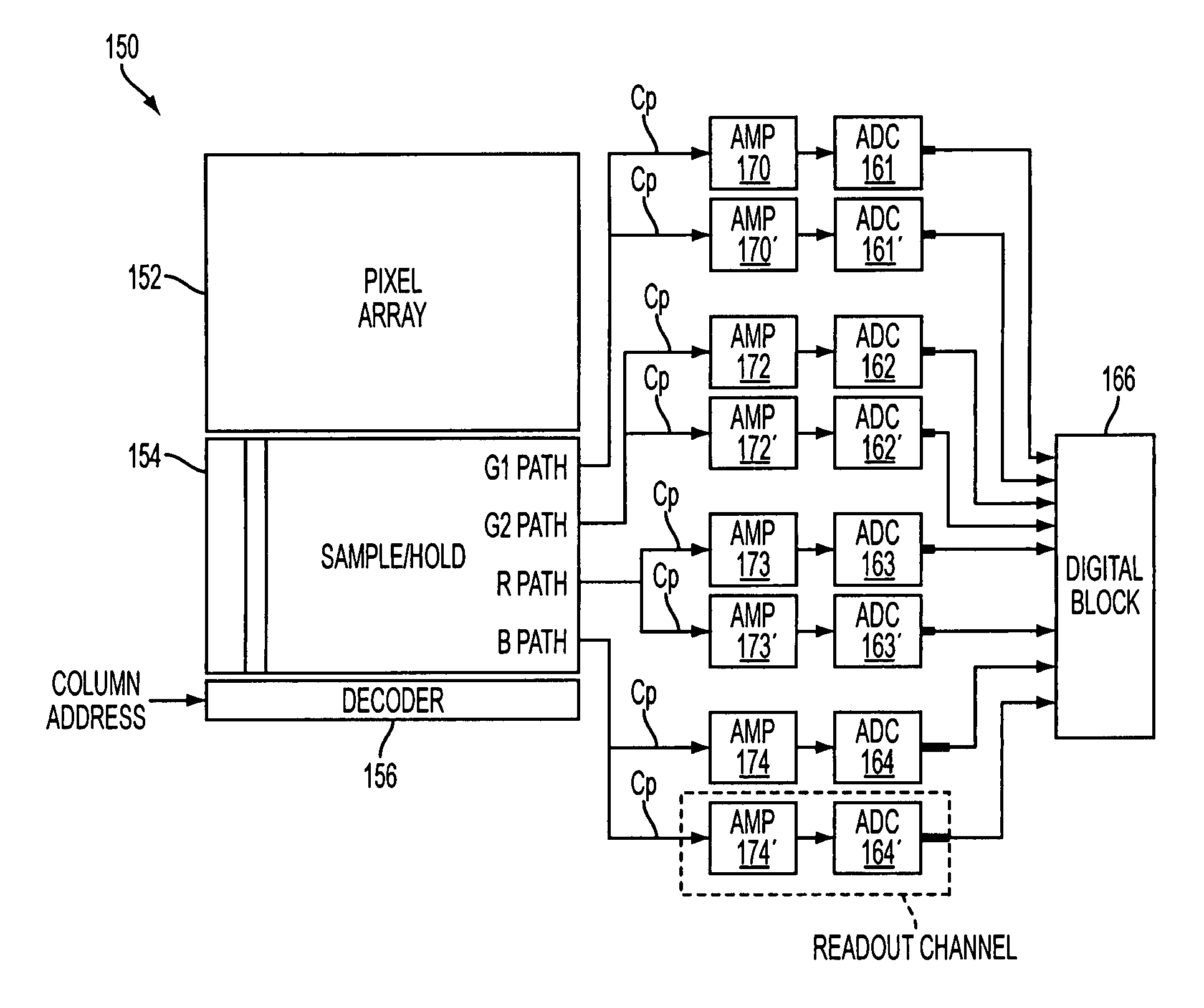
[0025]The invention generally relates to parallel readout of columns in a pixel...


PUM


Abstract

An imaging device with readout chain circuitry that uses multiple analog-to-digital converters and amplifiers, which are similarly calibrated using a stitching technique, to readout each color of a column and mitigate the possibility of a boundary effect.

Description

FIELD OF THE INVENTION[0001]The invention relates to an image sensor and more particularly to a readout technique and circuit for parallel readout of signals from a pixel array.BACKGROUND OF THE INVENTION[0002]Imaging devices, including charge coupled devices (CCD) and complementary metal oxide semiconductor (CMOS) imagers, are commonly used in photo-imaging applications.[0003]A CMOS imager circuit includes a focal plane array of pixels, each one of the cells including a photosensor, for example, a photogate, photoconductor or a photodiode overlying a substrate for accumulating photo-generated charge in the underlying portion of the substrate. Each pixel has a readout circuit that includes at least an output field effect transistor formed in the substrate and a charge storage region formed on the substrate connected to the gate of an output transistor. The charge storage region may be constructed as a floating diffusion region. Each pixel may include at least one electronic device s...

Claims


Application Information

Patent Timeline
Patent Type & Authority Patents(United States)
IPC IPC(8): H01L27/00H03F3/08H04N3/14
CPCH04N3/1593H04N5/3653H04N5/3742H04N5/378H04N25/41H04N25/672H04N25/767H04N25/75
Inventor LEE, CHIAJEN M.CHO, KWANG-BO
Owner APTINA IMAGING CORP
Why Eureka
Try Eureka