
Micro optical bench structure

a bench structure and optical technology, applied in semiconductor lasers, instruments, record information storage, etc., can solve the problems of product characteristics and reproducibility reduction, and achieve the effects of reducing production costs, reproducibility and reliability, and reducing the number of steps in the manufacturing process

Inactive Publication Date: 2008-11-25
SAMSUNG ELECTRONICS CO LTD
View PDF9 Cites 5 Cited by
  • Summary
  • Abstract
  • Description
  • Claims
  • Application Information

AI Technical Summary

Benefits of technology

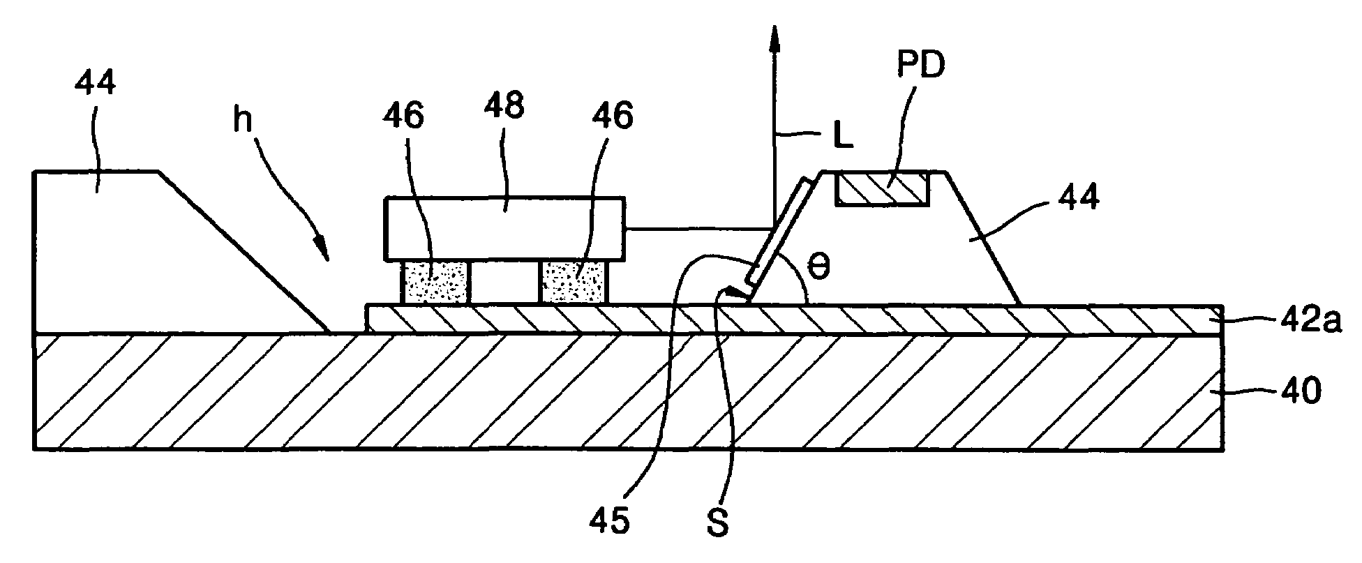
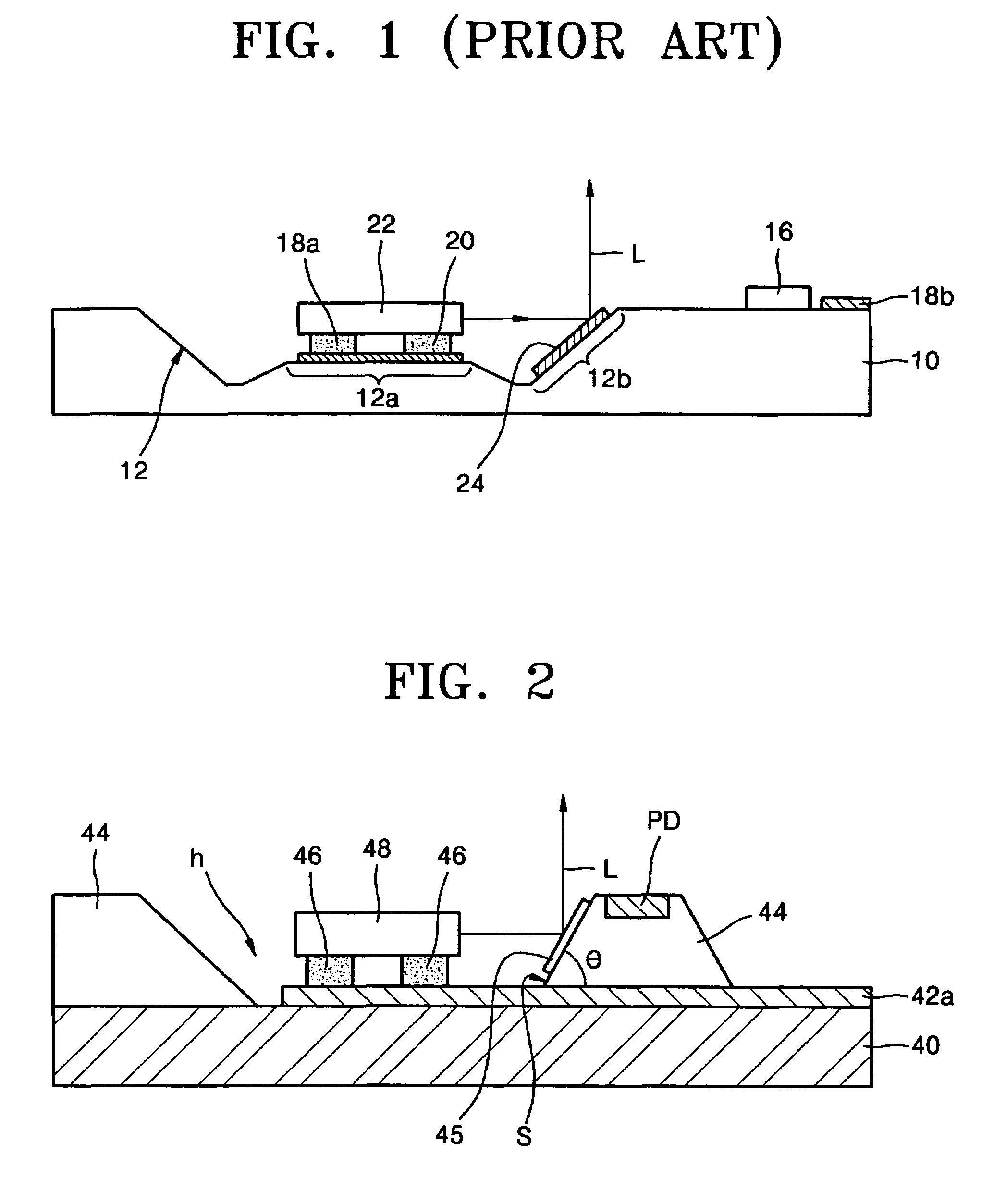
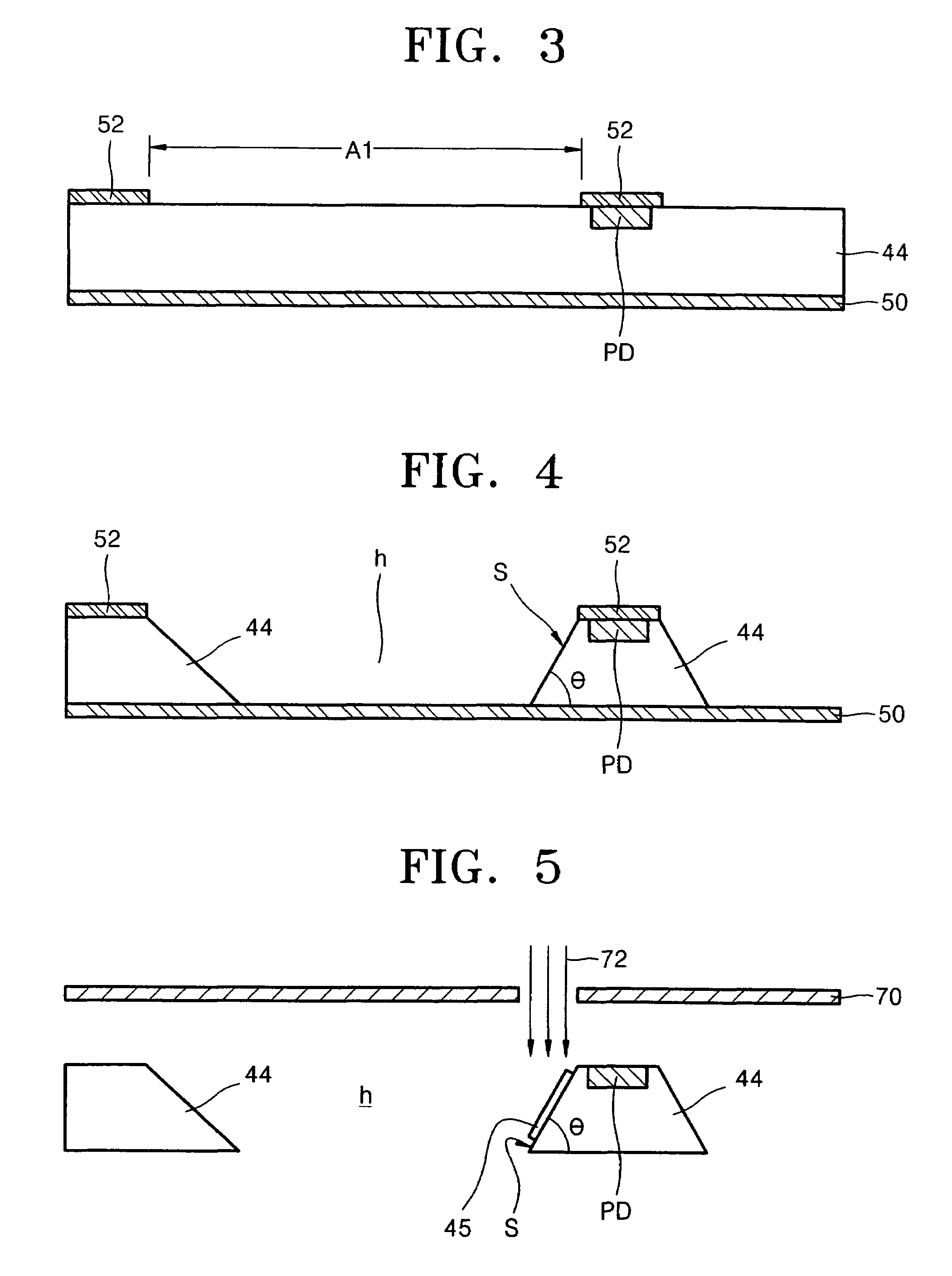
The present invention provides a micro optical bench structure and a method of manufacturing it that can simplify the process, increase reproducibility, and improve reliability. The structure includes a lower substrate, an upper substrate, and a first optical device installed on the lower substrate. The upper substrate has a through-hole exposing the lower substrate, and a reflection unit is installed on the inner surface of the through-hole. The first and second substrates are bonded together to form the micro optical bench structure. The method of manufacturing the structure includes sequentially installing an electrode wire and a flip-chip bonding unit on the lower substrate, mounting a light emitting device on the flip-chip bonding unit, forming a through-hole in the second substrate, installing a reflection unit on the inner surface of the through-hole, and bonding the first and second substrates such that the light emitting device is positioned within the through-hole.

Problems solved by technology

The conventional optical bench structure has a drawback in that some product characteristics, for example, reproducibility can be reduced due to a complicated process.

Method used


Image

  • Micro optical bench structure
  • Micro optical bench structure
  • Micro optical bench structure

Examples


Embodiment Construction

[0036]The present invention will now be described more fully with reference to the accompanying drawings, in which exemplary embodiments of the invention are shown. The invention may, however, be embodied in many different forms and should not be construed as being limited to the exemplary embodiments set forth herein; rather, these embodiments are provided so that this disclosure will be thorough and complete, and will fully convey the concept of the invention to those skilled in the art. In the drawings, the thicknesses of layers and regions are exaggerated for clarity. It will also be understood that when a layer is referred to as being “on” another layer or substrate, it can be directly on the other layer or substrate, or intervening layers may also be present. Like reference numerals in the drawings denote like elements, and thus their description will be omitted.

[0037]Consistent with the present invention, a micro optical bench structure and a method of manufacturing the same ...


PUM

PropertyMeasurementUnit
angleaaaaaaaaaa
slope angleaaaaaaaaaa
structureaaaaaaaaaa

Abstract

A micro optical bench structure and a method of manufacturing a micro optical bench structure are provided. The micro optical bench structure includes: a lower substrate; an upper substrate which is bonded to the lower substrate, and has a through-hole for exposing the lower substrate; and a first optical device which is installed at the lower substrate, and units relating to the first optical device.

Description

BACKGROUND OF THE INVENTION[0001]This application claims the priority of Korean Patent Application No. 10-2004-0002251, filed on Jan. 13, 2004, in the Korean Intellectual Property Office, the disclosure of which is incorporated herein in its entirety by reference.[0002]1. Field of the Invention[0003]The present invention relates to an optical pickup device and a method of manufacturing the same and, more particularly, to a micro optical bench structure having a light emitting device such as a laser diode and a light receiving device such as a photo diode and a method of manufacturing the same.[0004]2. Description of the Related Art[0005]When information is written on a disc-type optical recording medium such as Compact Disks (CDs) or Digital Versatile Disks (DVDs), an inputted electric signal is converted into a laser beam and irradiated on the optical recording medium. Additionally, when information recorded in the optical recording medium is read, the laser beam, which is reflecte...

Claims


Application Information

Patent Timeline
Patent Type & Authority Patents(United States)
IPC IPC(8): H01L27/15H01S5/022G02B6/12G11B7/12G11B7/123G11B7/135G11B7/1362G11B7/22
CPCG11B7/1205G11B7/1362G11B7/22H01S5/02248H01S5/02292G11B7/123H01L2224/81H01S5/02255H01S5/02325B27K5/065B44C1/00
Inventor KIM, YONG-SUNGCHUNG, SEOK-WHANYOU, JAO-HOCHOI, HYUNGHWANG, WOONG-LIN
Owner SAMSUNG ELECTRONICS CO LTD
Learn More