Semiconductor storage device

a technology of a storage device and a semiconductor, applied in the direction of instruments, coding, code conversion, etc., can solve the problem that the error correction bits cannot be generated, and achieve the effect of enhancing the speed of error correction bits generation

Inactive Publication Date: 2008-11-25
RENESAS ELECTRONICS CORP
View PDF11 Cites 19 Cited by
  • Summary
  • Abstract
  • Description
  • Claims
  • Application Information

AI Technical Summary

Benefits of technology

[0013]In addition, in case the number of actual input data is equal to the number of data bits necessary for ECC processing, the speed of generation of the error correction bits may be enhanced.

Problems solved by technology

However, in case the number of bits required for error correction is 256 bits and write data is less than 256 bits, such as one byte, or in case data is written in a burst but the transfer data is masked, there is raised a problem that error correction bits cannot be generated.

Method used


Image

  • Semiconductor storage device
  • Semiconductor storage device
  • Semiconductor storage device

Examples


first embodiment

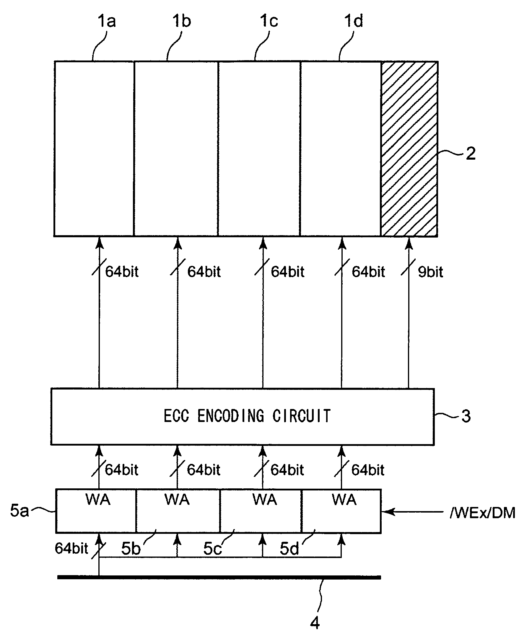
[0030]FIGS. 1 to 3 illustrate a semiconductor storage device according to the present invention.

[0031]FIG. 1 illustrates data write operation and ECC operation of a semiconductor storage device according to the first embodiment of the present invention. In FIG. 1, the process of generating 9 error correction bits, responsive to 256-bit data, and storing the 256-bit data in a cell array core block and in an ECC code cell, are schematically illustrated.

[0032]The semiconductor storage device according to the first embodiment of the present invention, includes a plural number of cell array core blocks 1a to 1d, an ECC code cell 2, an ECC encoding circuit 3, a write data bus 4 and write amplifiers 5a to 5d. The cell array core blocks 1a to 1d are collectively termed a cell array core. The operation of the device is now explained in detail.

[0033]The semiconductor storage device according to the present embodiment, four 64-bit data, that is, first to fourth consecutive write data (64 bit) ...

third embodiment

[0055]In the third embodiment, as indicated by “*2” in FIG. 13, the late write function is used to render invisible the wait time until data corresponding to the burst length is ready. The data D0 to D3 are sequentially entered from time t4 until time t8.

[0056]At the timing t4, write data Dn-8 to Dn-5, entered during the previous write cycle, is transferred from the register (time period (5) in FIG. 13). As a parallel operation, dummy read is carried out from the memory cells corresponding to the address entered during the previous write cycle (time period (6) in FIG. 13).

[0057]At the timing t5, ECC encoding is carried out with the write data of the previous cycle and dummy read data corresponding to the write address of the previous cycle (time period (7) in FIG. 13).

[0058]At the timing t6, the resulting encoded data is written in the ECC cell (time period (8) in FIG. 13).

[0059]That is, by employing the late write function, the time interval from t5 until t8, which was a wait time ...


PUM


Abstract

Disclosed is a semiconductor storage device including an error correction bit generating circuit for generating error correction bits from data composed of a predetermined number of bits. The semiconductor storage device is featured by generating error correction bits using data supplied from outside and data stored in memory cells. More specifically, the semiconductor storage device includes a write amplifier for receiving first data supplied from outside, a first group of memory cells having stored second data corresponding to an address pertinent to the first data, an error correction bit generating circuit for generating error correction bits based on the first and second data, a second group of memory cells for storage of the first data, and a third group of memory cells for storing the error correction bits.

Description

FIELD OF THE INVENTION[0001]The present invention relates to a semiconductor storage device and, more particularly to a semiconductor storage device having an ECC (error correction code) function.BACKGROUND OF THE INVENTION[0002]In e.g. a server system, where extremely high reliability is required, memory errors may be a cause for a fatal system fault. For avoiding the problem of memory errors, such a memory having an error correcting function has been developed. This memory is able to detect the presence of a memory error, specify the location where an error has occurred, and to correct the error.[0003]The memory having such error correcting function, or the so-called ECC function, adopts for example a Hamming code as check bits. The number of check bits is correlated with the data bus width, such that, in case the data bus width is N bits, the number of the check bits may be found by taking a log of N with a base of 2 and by adding 2 to the so obtained log. Thus, in a memory havin...

Claims


Application Information

Patent Timeline
Patent Type & Authority Patents(United States)
IPC IPC(8): G11C29/00G11C29/42G06F11/10G11C7/00G11C11/401G11C11/409G11C11/419H03M13/00
CPCG06F11/1008G06F11/108
Inventor TAKAHASHI, HIROYUKI
Owner RENESAS ELECTRONICS CORP
Why Eureka
Try Eureka