

Light emitting diode package having dual lens structure for lateral light emission
a technology of light-emitting diodes and lens structures, which is applied in the direction of instruments, lighting and heating apparatus, optical elements, etc., can solve the problems of difficult molds, difficult to precisely form connection parts, and degrade the optical characteristics of led packages, so as to achieve efficient installation and facilitate manufacturing
- Summary
- Abstract
- Description
- Claims
- Application Information
AI Technical Summary
Benefits of technology
Problems solved by technology
Method used
Image

Examples
Embodiment Construction
[0039]Preferred embodiments of the present invention will now be described in detail with reference to the accompanying drawings.
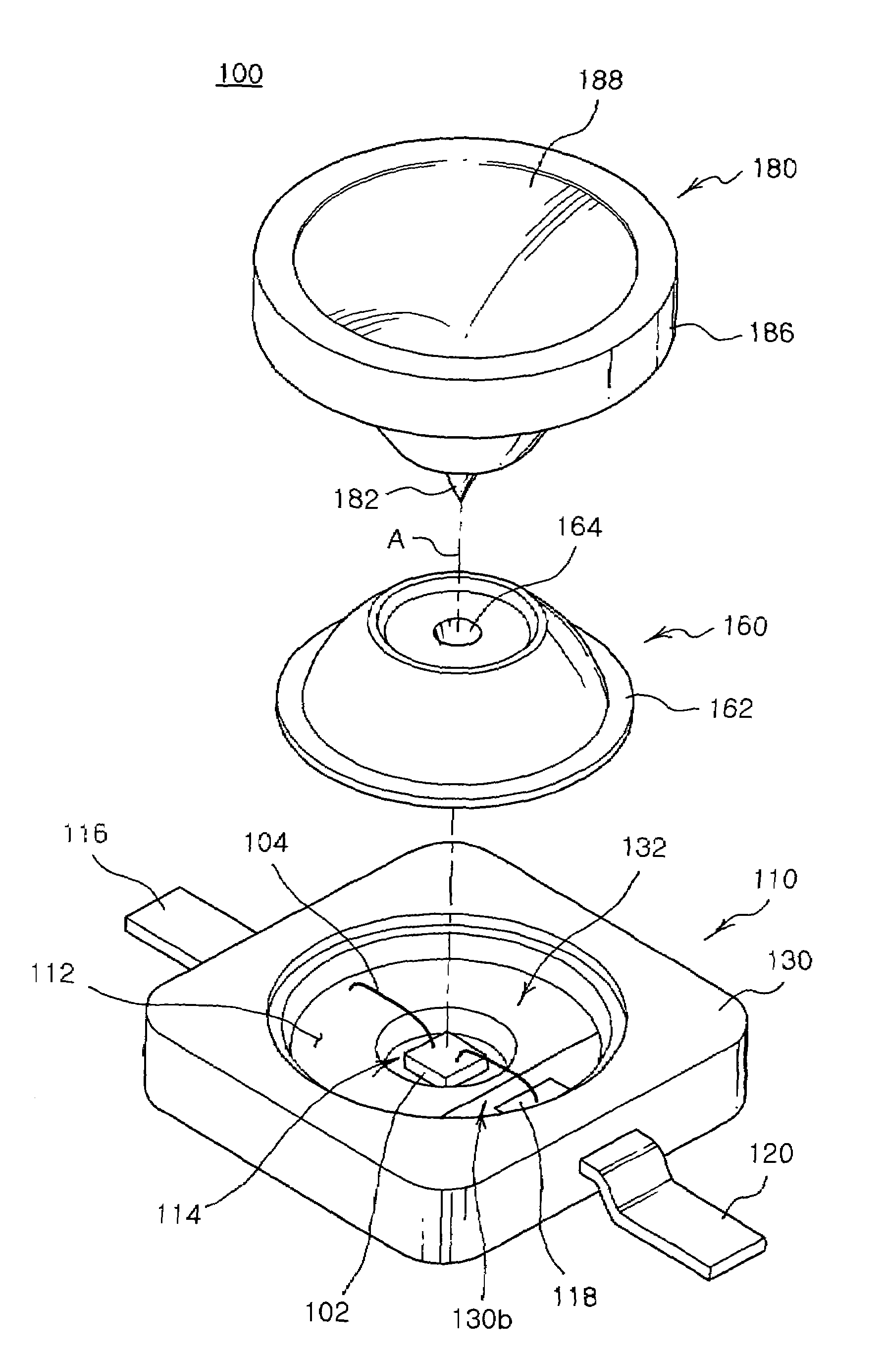
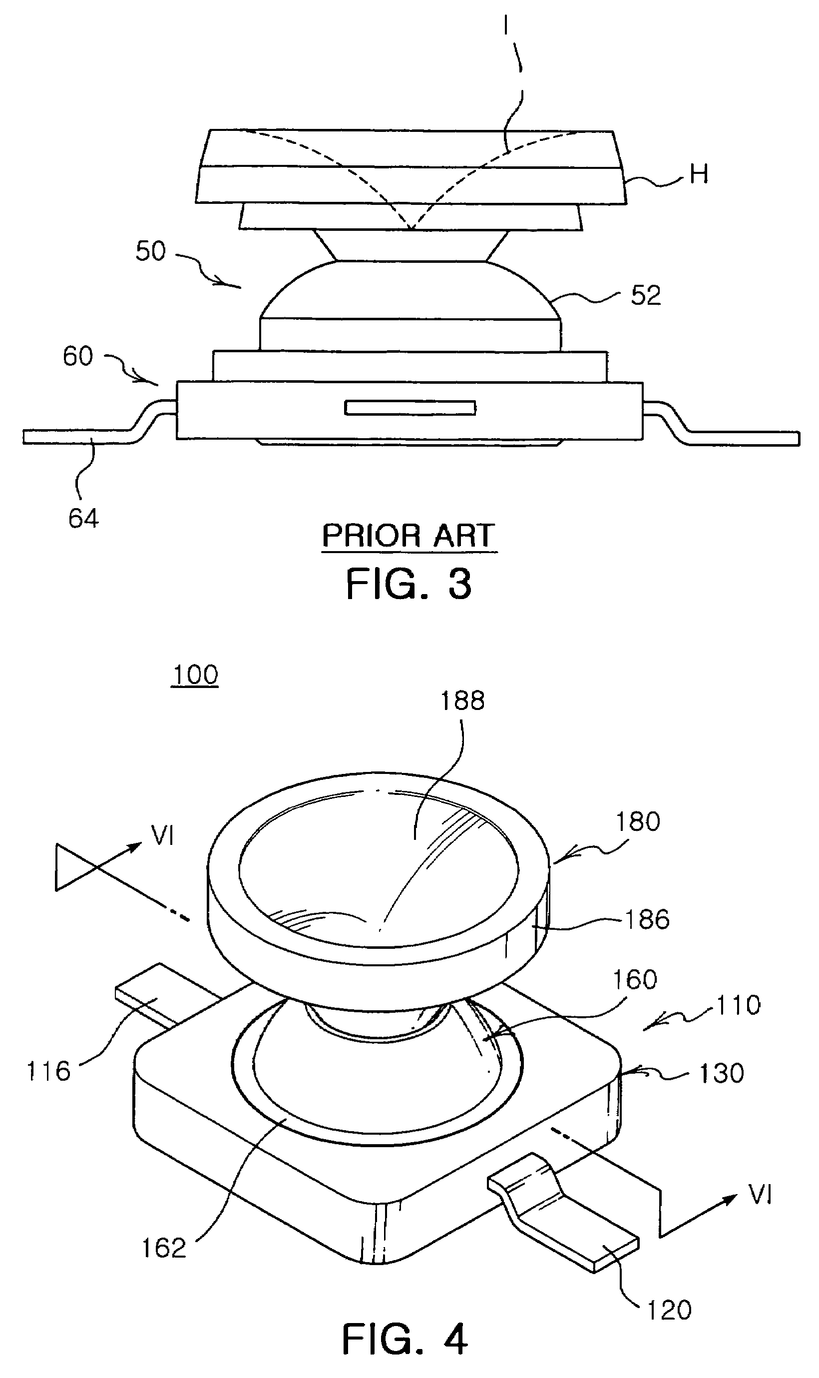
[0040]FIG. 4 is a perspective view illustrating an LED package having a dual lens structure according to the present invention, FIG. 5 is an exploded view of the LED package shown in FIG. 4, FIG. 6 is a sectional view taken along line 6-6 of FIG. 4, and FIG. 7 is an exploded view of the LED package shown in FIG. 6.
[0041]Referring to FIGS. 4 to 7, the LED package 100 having a dual lens structure according to the present invention includes a lower structure 110, a lower lens 160 and an upper lens 180.
[0042]The lower structure 110 includes a heat conducting part 112, a lead 120, a package body 130 holding parts of the heat conducting part 112 and the lead 120, and a transparent encapsulant 140.
[0043]The package body 130 is generally made of resin that is opaque or has high reflectivity. The package body 130 has a recess 132 surrounded by a stepped lower lens ...
PUM
 Abstract
Description
Claims
Application Information