Method for producing and epitaxial substrate for compound semiconductor light-emitting device

a light-emitting device and semiconductor technology, applied in the direction of semiconductor devices, basic electric elements, electrical devices, etc., can solve the problems of poor crystallinity of the protective layer, insufficient thermal stability, and lowered injection efficiency of holes into the light-emitting layer structure, so as to achieve excellent protective performance, increase the injection efficiency of holes, and improve the effect of thermal stability

Inactive Publication Date: 2008-12-02
SUMITOMO CHEM CO LTD
View PDF13 Cites 8 Cited by
  • Summary
  • Abstract
  • Description
  • Claims
  • Application Information

AI Technical Summary

Benefits of technology

[0014]Another object of the present invention is to provide an epitaxial substrate for compound semiconductor light-emitting device, a method for producing the same and a light-emitting device, which enable highly efficient injection of holes into the light-emitting layer structure without impairing the protective layer's ability to protect the light-emitting layer structure.
[0015]The present invention achieves the foregoing objects by inserting between the protective layer and the p-type layer an intermediate layer so as to ensure excellent protective performance even when the protective layer is made thin and to increase hole injection efficiency and enhance light-emission efficiency by bringing the p-type layer close to the light-emitting layer structure.

Problems solved by technology

In contrast, the thermal stability of an InGaAlN-system mixed crystal (containing In), though differing with the InN mixed crystal ratio, is not so good, so this compound semiconductor is generally grown at a relatively low temperature of around 800° C. As a result, the InGaAlN-system mixed crystal growth layer constituting an important growth layer of the light-emitting layer structure of a visible-light-region light-emitting device has to be grown at a low temperature and is therefore frequently inadequate in thermal stability.
However, when a protective layer containing Al is grown at the same temperature as that at which the light-emitting layer structure was grown, the crystallinity of the protective layer is not good.
The injection efficiency of holes into the light-emitting layer structure is therefore lowered and it becomes difficult to achieve high light-emission efficiency.
Moreover, owing to the fact that the performance of the AlGaN layer as a protective layer declines with decreasing Al content, the GaN protective layer of the prior art method (b) also has to be increased in thickness, so that no improvement in light-emission efficiency can be expected.

Method used


Image

  • Method for producing and epitaxial substrate for compound semiconductor light-emitting device
  • Method for producing and epitaxial substrate for compound semiconductor light-emitting device
  • Method for producing and epitaxial substrate for compound semiconductor light-emitting device

Examples


example 1

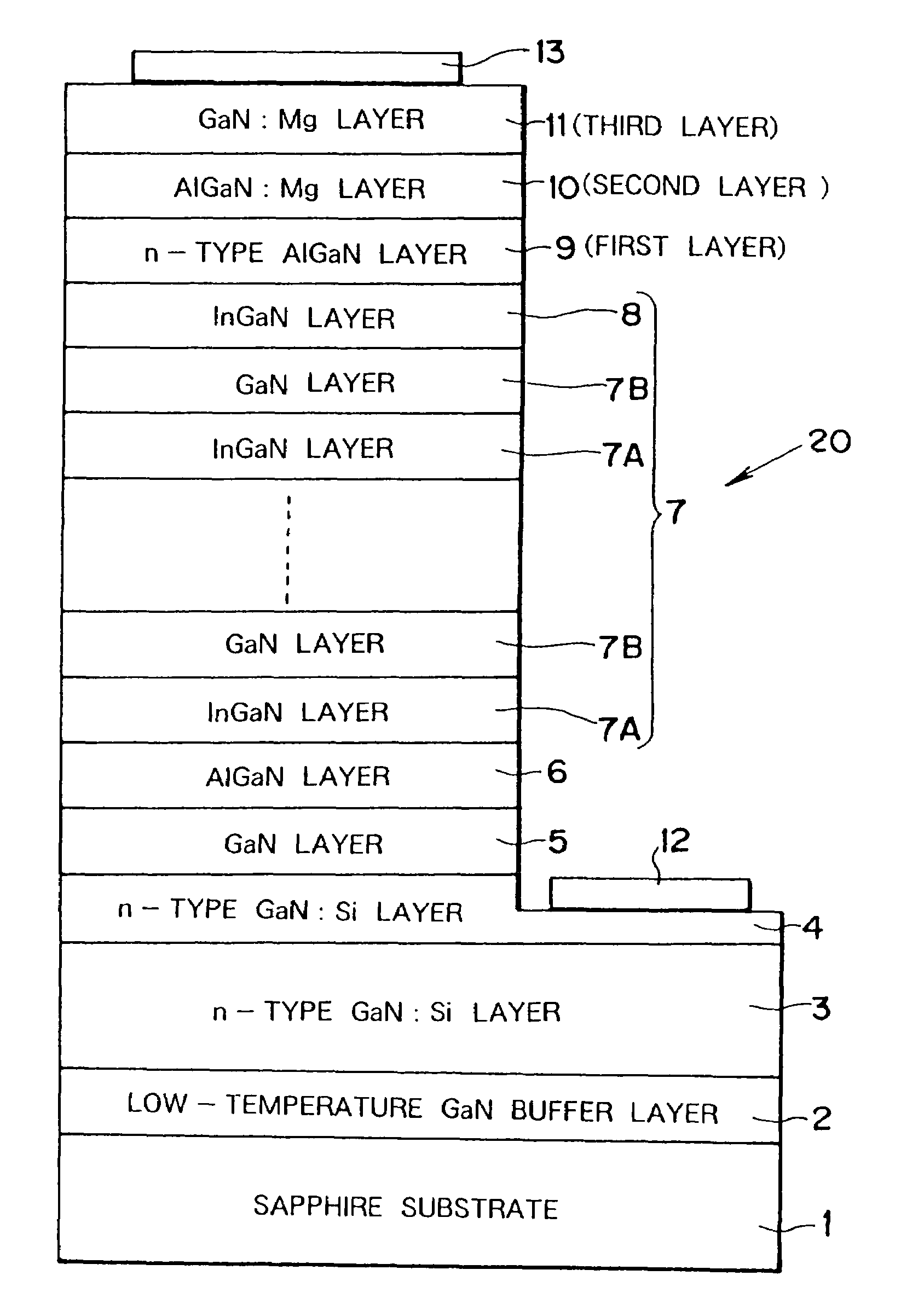
[0060]The multilayer light-emitting device shown in FIG. 1 was fabricated as explained in the following by using the MOVPE process to grow crystal layers on a sapphire substrate. First, an epitaxial substrate for a compound semiconductor light-emitting device was fabricated starting with a sapphire substrate 1. The sapphire substrate 1 was set in an MOVPE growth furnace and a thin layer of GaN was grown on the sapphire substrate 1 as the low-temperature GaN buffer layer 2 using NH3, MO (TMG) and silane as source gases and H2 as carrier gas. The n-type GaN:Si layer 3 was then grown at 1040° C.

[0061]The sapphire substrate 1 was then once removed from the MOVPE growth furnace, subjected to a prescribed inspection, and returned to the MOVPE growth furnace. The n-type GaN: Si layer 4 was then grown on the n-type GaN : Si layer 3 at a growth temperature of 1040° C. using NH3, MO (TMG, TMA and TMI) and silane as source gases and H2 as carrier gas. The undoped GaN layer 5 was next grown on ...

examples 9-16

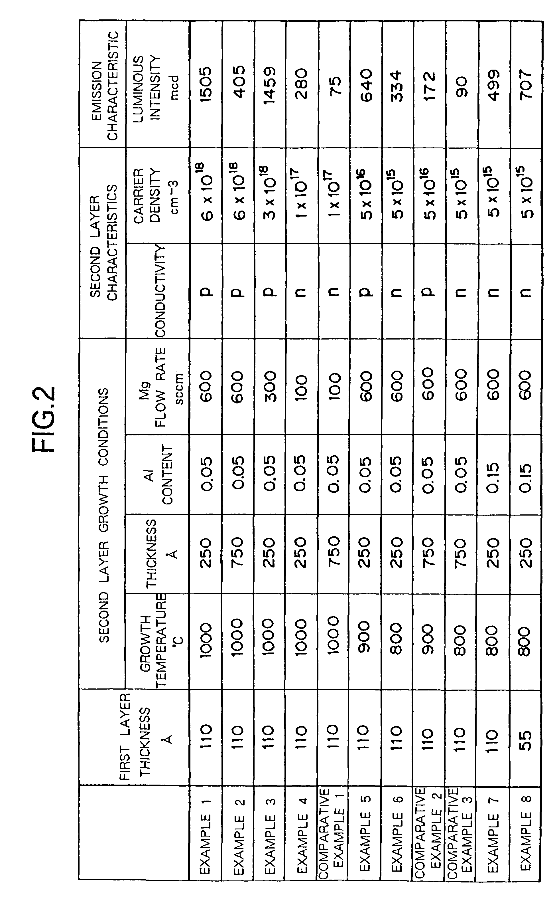
[0076]Examples 9 to 16 of the present invention will now be explained. In Examples 9 to 16, light-emitting devices were fabricated under the same conditions as in Example 1 except that an AlGaN layer 9 having an Al content of 0 was used as the first layer, i.e., the first layer was formed as an n-type GaN layer of 180 Å thickness, and the AlGaN: Mg (second) layer 10 was formed under growth conditions differing variously in growth temperature, Al content and Mg flow rate.

[0077]FIG. 4 shows growth conditions and characteristics of each of the light-emitting devices fabricated in Examples 9 to 16, specifically second layer growth conditions (growth temperature (° C.), thickness ( Å), Al content and Mg flow rate (sccm)), characteristics of the second layer (conductivity type and carrier density (cm−3), and measured emission characteristic (luminous intensity (mcd)). In Examples 9-16, the second layer was grown at a growth temperature (° C.) equal to or higher than the value obtained by ...


PUM


Abstract

In order to improve light-emission efficiency without degrading protection performance of a light-emitting layer structure a three p-type layer structure composed of first to third layers is provided in contact with a light-emitting layer structure. The first layer is an n-type AlGaN layer that serves as a protective layer, the third layer is a GaN:Mg layer that serves as a contact layer and the second layer is an AlGaN:Mg layer formed between these layers as an intermediate layer. The provision of the intermediate layer enables an InGaN layer to be thoroughly protected from heat during growth of layers above even if the n-type AlGaN layer is made thin, whereby the GaN:Mg layer can be brought near the light-emitting layer structure to enhance the efficiency of hole injection into the light-emitting layer structure and thus increase the light-emission efficiency.

Description

[0001]The present invention is a Divisional of application Ser. No. 10 / 614,062, filed on Jul. 8, 2003 now U.S. Pat. No. 7,098,484, the entire contents of which are hereby incorporated by reference and for which priority is claimed under 35 U.S.C. § 120.BACKGROUND OF THE INVENTION[0002]1. Field of the Invention[0003]This invention relates to an epitaxial substrate for a compound semiconductor light-emitting device composed of stacked layers of nitride-system III-V Group compound semiconductor thin film, a method for producing the same, and a light-emitting device.[0004]2. Background Art[0005]III-V Group compound semiconductors represented by the general formula InxGayAlzN (where x+y+z=1, 0≦x≦1, 0≦y≦1, 0≦z≦1) are known as materials for purple, blue and green light-emitting diodes and blue and green laser diodes. In the following, the symbols x, y and z appearing in this general formula are sometimes used to denote InN mixed crystal ratio, GaN mixed crystal ratio and AlN mixed crystal ...

Claims


Application Information

Patent Timeline
Patent Type & Authority Patents(United States)
IPC IPC(8): H01L21/00H01L33/14H01L33/32
CPCH01L33/32H01L33/14
Inventor YAMANAKA, SADANORITSUCHIDA, YOSHIHIKOONO, YOSHINOBUIYECHIKA, YASUSHI
Owner SUMITOMO CHEM CO LTD
Why Eureka
Try Eureka