Fast and compact SCR ESD protection device for high-speed pins

a protection device and high-speed pin technology, applied in the direction of emergency protective circuit arrangement, emergency protective device details, emergency protective arrangements for limiting excess voltage/current, etc., can solve the problem of slowness of scr devices, ineffective against charge-device-model esd which is much faster, etc. problem, to reduce the delay time for turning on pnp bipolar transistors, reduce the p-well and n-well resistance of scrs, and reduce the breakdown current of zen

Inactive Publication Date: 2008-12-30
ALTERA CORP
View PDF4 Cites 30 Cited by
  • Summary
  • Abstract
  • Description
  • Claims
  • Application Information

AI Technical Summary

Benefits of technology

[0005]A preferred embodiment of the present invention comprises a pair of SCR devices connected in antiparallel between first and second nodes. Each SCR device comprises an NPN and a PNP bipolar transistor. Reverse-biased Zener diodes are used for triggering the NPN bipolar transistor in each SCR device when it breaks down in an ESD event. Advantageously, additional Zener diodes are provided for pre-charging the PNP transistor of each SCR device at the same time, thereby reducing the delay time for turning on the PNP bipolar transistor. In addition, the breakdown current of the Zener diodes is preferably maximized by reducing the P-well and N-well resistance of the SCRs. This is achieved by connecting external resistances between the base of each bipolar transistor and the node to which the emitter of the transistor is connected.

Problems solved by technology

Unfortunately, SCR devices are known to be slower than bipolar transistors.
As a result, while SCR devices are capable of protecting integrated circuits against the Human-Body-Model (HBM) ESD, they are not effective against the Charge-Device-Model (CDM) ESD which is much faster.

Method used


Image

  • Fast and compact SCR ESD protection device for high-speed pins
  • Fast and compact SCR ESD protection device for high-speed pins
  • Fast and compact SCR ESD protection device for high-speed pins

Examples


Embodiment Construction

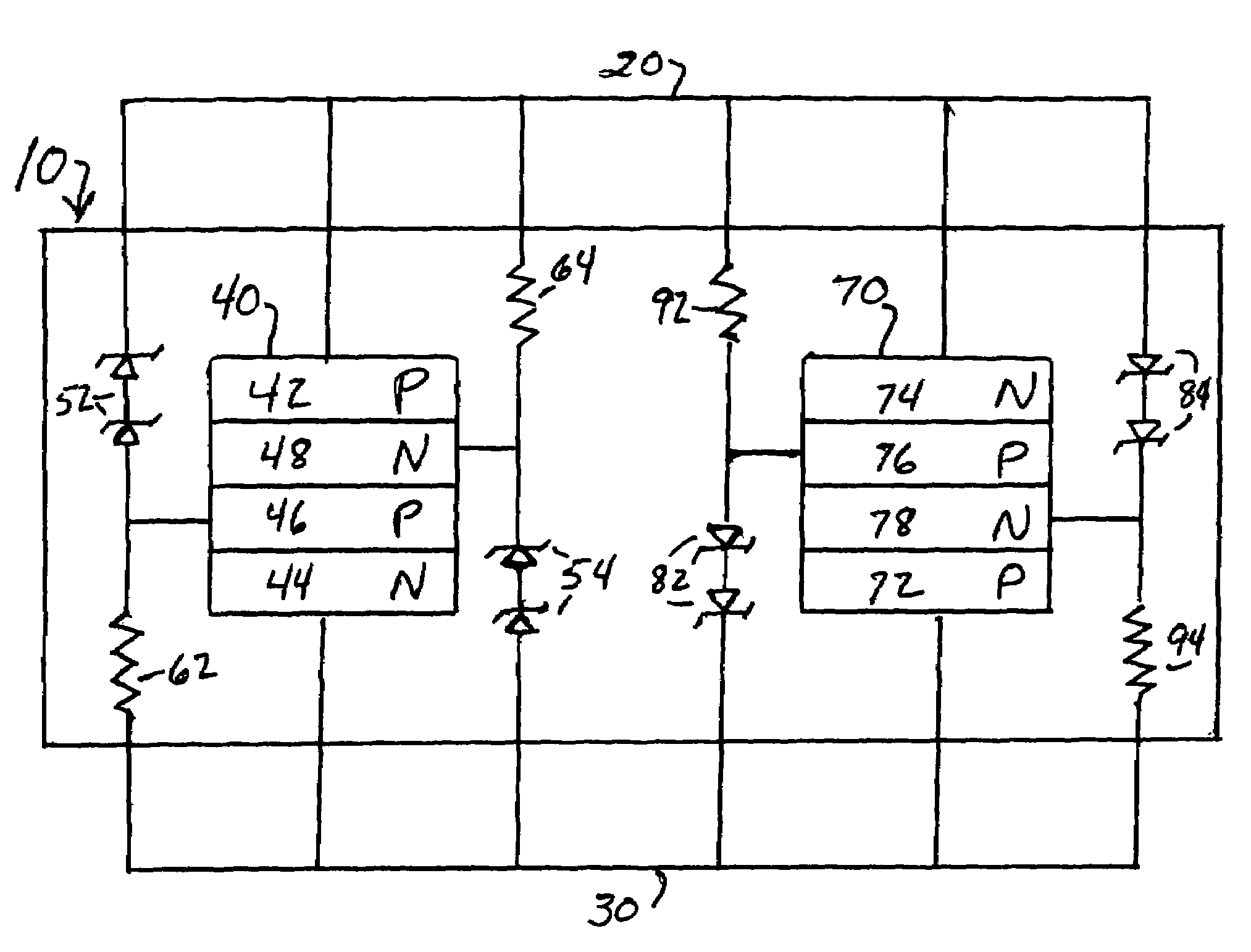
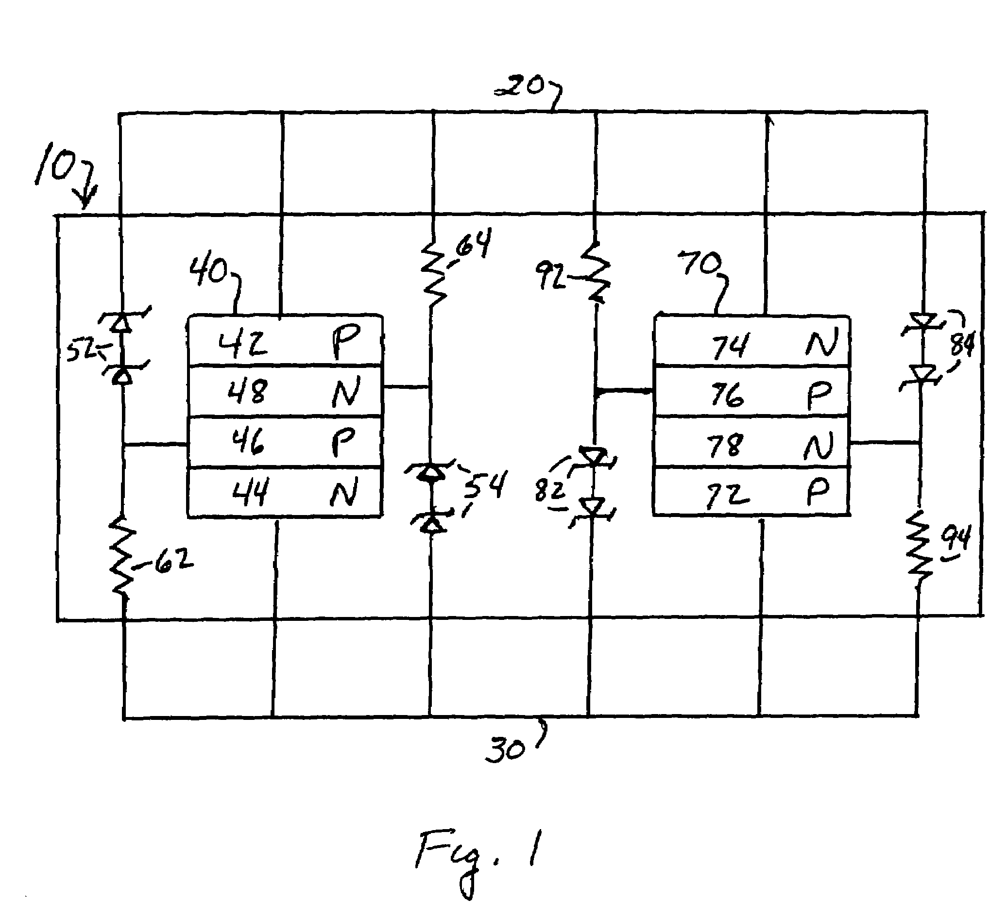
[0010]FIG. 1 depicts an electrostatic discharge (ESD) protection device 10 for discharging either positive or negative electrostatic pulses on a first node 20 by rapidly connecting them to a second node 30 that typically is connected to ground. Device 10 comprises first and second PNPN devices 40, 70. Each PNPN device has an anode, a cathode, and first and second gates. For PNPN device 40, these elements are numbered 42, 44, 46, 48. For PNPN device 70, these elements are numbered 72, 74, 76, 78. As shown in FIG. 1, anode 42 of the first device is connected to first node 20 and cathode 44 is connected to second node 30. Anode 72 of the second device is connected to second node 30 and cathode 74 is connected to first node 20.

[0011]One or more Zener diodes 52 is connected between first gate 46 of the first PNPN device and first node 20; and one or more Zener diodes 54 is connected between second gate 48 and second node 30. For purposes of illustration, two pairs of series connected dio...


PUM


Abstract

A pair of SCR devices connected in antiparallel between first and second nodes. Each SCR device comprises an NPN and a PNP bipolar transistor. Reverse-biased Zener diodes are used for triggering the NPN bipolar transistor in each SCR device when it breaks down in an ESD event. Advantageously, additional Zener diodes are provided for pre-charging the PNP transistor of each SCR device at the same time, thereby reducing the delay time for turning on the PNP bipolar transistor. In addition, the breakdown current of the Zener diodes is preferably maximized by reducing the P-well and N-well resistance of the SCRs. This is achieved by connecting external resistances between the base of each bipolar transistor and the node to which the emitter of the transistor is connected.

Description

CROSS REFERENCE TO RELATED APPLICATIONS[0001]This application is a continuation-in-part of application Ser. No. 10 / 938,102, filed Sep. 10, 2004, now U.S. Pat. No. 7,342,282 for “Compact SCR Device and Method for Integrated Circuits.” It is also a continuation-in-part of application Ser. No. 10 / 882,874, filed Jun. 30, 2004 now U.S. Pat. No. 7,195,958 for “Methods of Fabricating ESD Protection Structures,” which application is a divisional of application Ser. No. 10 / 298,104, filed Nov. 14, 2002, now U.S. Pat. No. 6,777,721 for “SCR Device for ESD Protection.” The '102 and '874 applications and the '721 patent are incorporated by reference herein in their entireties.BACKGROUND OF THE INVENTION[0002]Silicon-Controlled-Rectifier (SCR) devices are widely used for electrostatic discharge (ESD) protection because they have smaller size, lower holding voltage and lower capacitance than bipolar transistors. The smaller size is due to the higher current-carrying capability compared to bipolar ...

Claims


Application Information

Patent Timeline
Patent Type & Authority Patents(United States)
IPC IPC(8): H02H9/00H02H1/00
CPCH01L23/60H01L27/0262H01L2924/0002H01L2924/00
Inventor HUANG, CHENG-HSIUNGSHIH, CHIH-CHINGO, HUGH SUNG-KILIU, YOWJUANG BILL
Owner ALTERA CORP
Why Eureka
Try Eureka