Dual mode single temperature trimming

a single-mode, trimming technology, applied in the field of circuit manufacturing, can solve problems such as error affecting circuits, variant electrical parameters, and source errors that cannot be removed by the designer of such a circui

Active Publication Date: 2008-12-30
NAT SEMICON CORP
View PDF4 Cites 27 Cited by
  • Summary
  • Abstract
  • Description
  • Claims
  • Application Information

AI Technical Summary

Problems solved by technology

There are several sources of error that contribute to non-ideal performance of circuits, such as bias circuits, and many of these sources of error cannot be removed by the designer of such a circuit.
Such sources of error include errors such as, but not limited to: mechanical stress during the manufacturing of the die; mechanical stress during packaging; and imperfections during manufacturing of the die resulting in variant electrical parameters.
Such sources of error affect the circuit in the form of process variation and mismatch.
Mismatch error only has meaning among devices in a single part.
In bias circuits for example, BJT process spread cannot be removed by design and is the traditional error source requiring trim.
All of these techniques take advantage of the fact that the BJT process spread on the VBE generating device produces a pure gain error.
A pure gain error results in the y-intercept of the signal versus temperature line remaining stable while the slope varies.
Likewise, the effect of manufacturing induced mismatch is often a critical source of error with respect to MOSFETs and resistors.
MOSFET mismatch in particular, is a large source of error in circuits, such as scalable bandgap circuits, which perform extensive mirroring using MOS devices.
In other words, mismatch error in MOS devices causes a pure offset error / absolute value error.
For example, in a bandgap generator, MOSFET mismatch can cause an error on the bandgap voltage that is effectively a consistent value (such as 10 millivolts too high or 20 millivolts too low) across a given temperature range.
A problem arises however, when both gain error and offset error exist simultaneously in a circuit.
With multiple simultaneous sources of error, some of which result in a gain error and some of which result in an offset error, present manufacturing techniques are unable to sort these errors apart from one another while the circuit remains at a single temperature.
Two techniques have been widely used to deal with such a problem, but each has drawbacks.
This technique however adds time, expense, and complexity to a manufacturing process.
Expense and complexity are added by creating a manufacturing line which must operate at two separate temperatures instead of one constant temperature.
Expense and complexity are also added by handling a circuit twice and performing extra measurements on a circuit under test and calibration.
One drawback is that trimming the process error of the BJT individually requires very precise temperature control of the manufacturing environment, often in excess of capability.
Ignoring other errors all together and trimming the BJT process variation by monitoring the bandgap voltage is also problematic because other error types may be exacerbated by the trim.
Another drawback is that dynamic element matching is a power hungry error reduction technique that causes the circuit to consume additional power.
Increased power consumption becomes even more apparent, when the output of a circuit needs to be sampled at a high frequency.
In such a case, the dynamic element matching techniques involved are also typically performed at a high frequency, which causes the circuit to consume even more power.
Yet another drawback is that such dynamic element matching techniques are often more complex to implement and manage compared to continuous DC signals.
However, these current methods often inadequately address the errors or else are costly, complex, and / or time consuming to implement.

Method used


Image

  • Dual mode single temperature trimming
  • Dual mode single temperature trimming
  • Dual mode single temperature trimming

Examples


Embodiment Construction

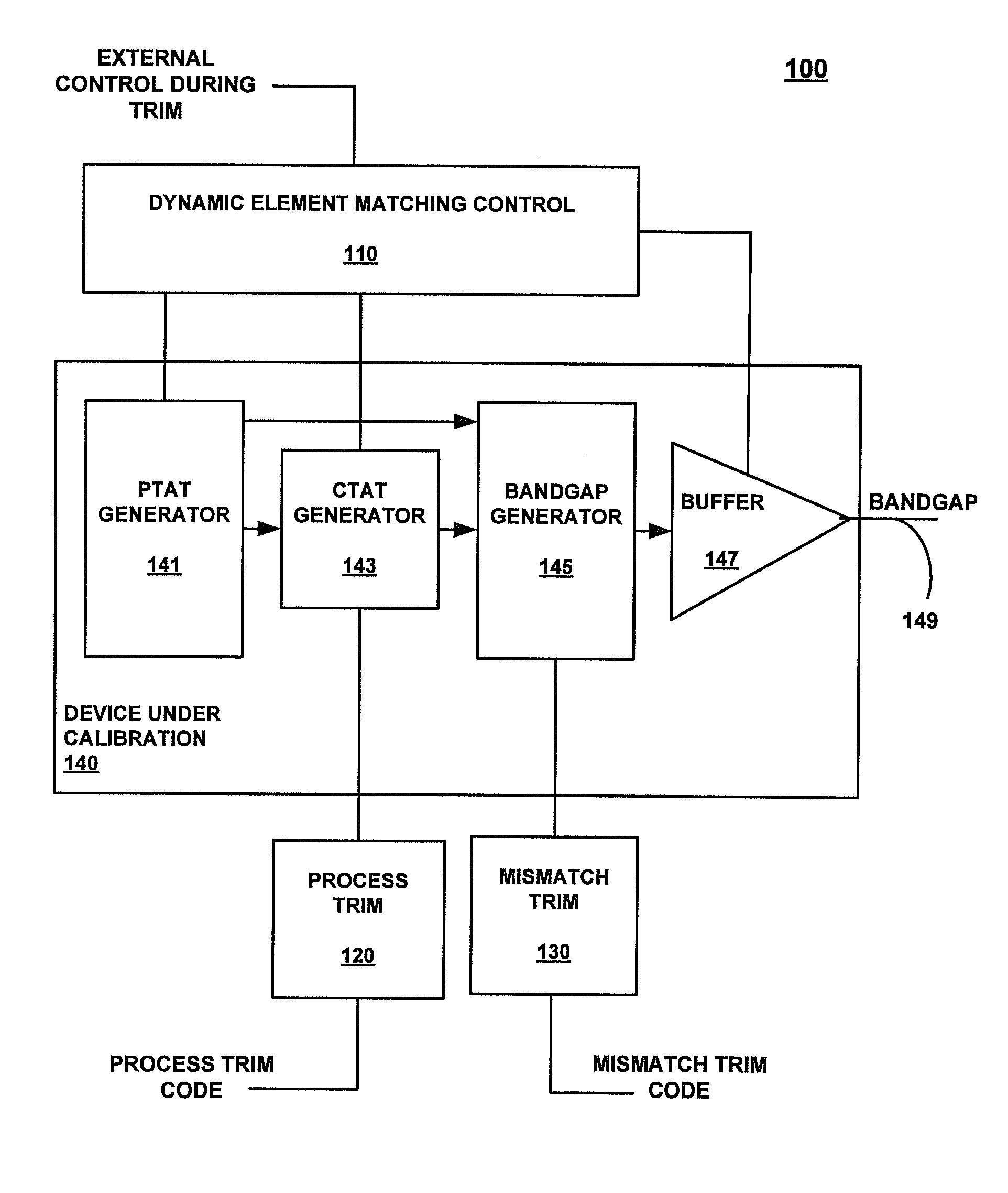
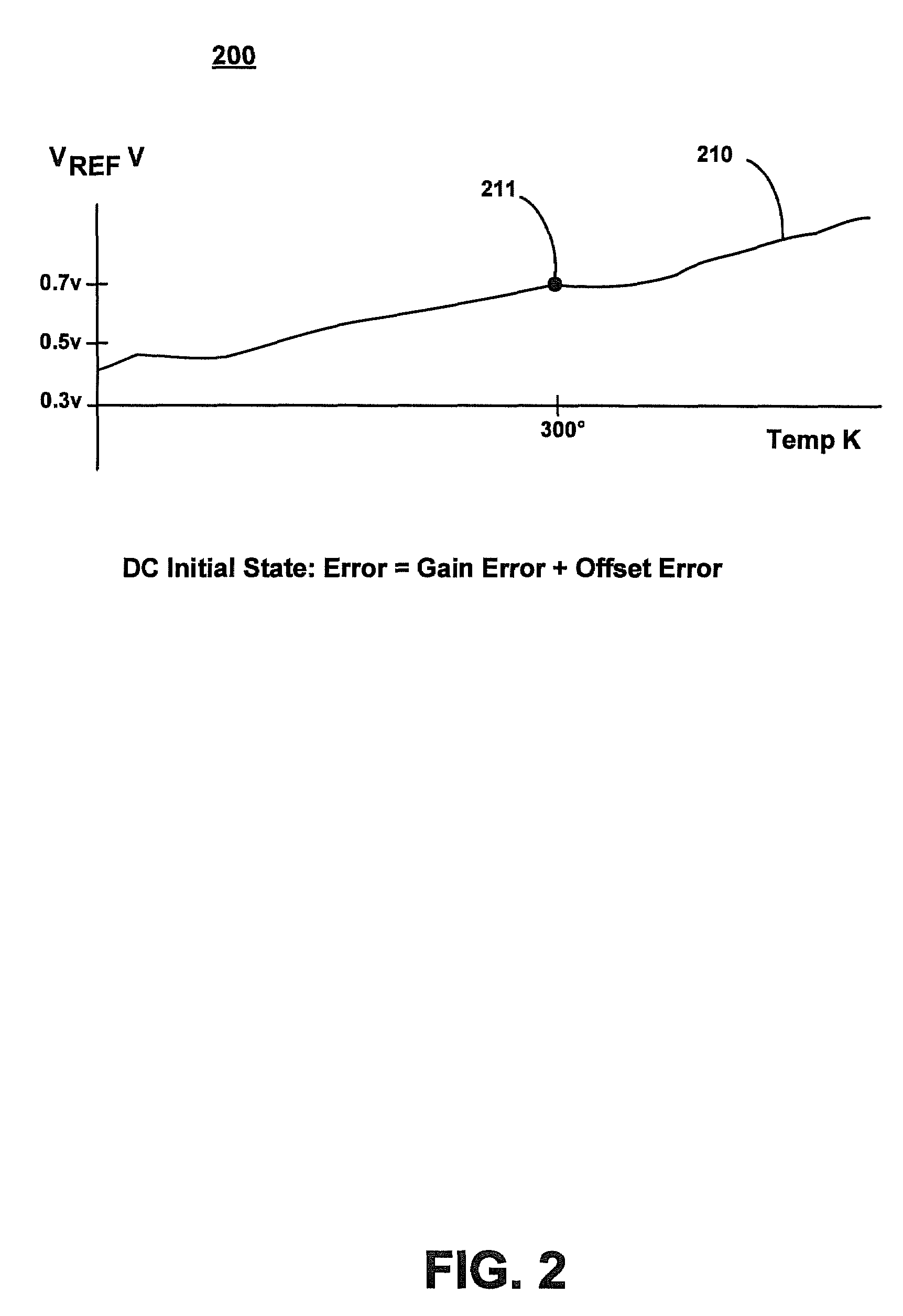
[0021]Reference will now be made in detail to embodiments of the present technology of dual mode single temperature trimming, examples of which are illustrated in the accompanying drawings. While the present technology will be described in conjunction with the preferred embodiments, it will be understood that they are not intended to limit the described technology to these embodiments. On the contrary, the present technology is intended to cover alternatives, modifications, and equivalent, which may be included within the spirit and scope of the technology as defined by the appended claims. Furthermore, in the following detailed description of the present technology, numerous specific details are set forth in order to provide a thorough understanding of the present technology. However, it will be recognized by one skilled in the art that the present technology may be practiced without these specific details or with equivalents thereof. In other instances, well-known methods, procedu...


PUM

PropertyMeasurementUnit
bandgap voltageaaaaaaaaaa
voltageaaaaaaaaaa

Abstract

In a system for performing a dual mode single temperature trim upon an electronic device to remove combined mismatch and process variation errors, a dynamic element matching control is configured for enabling dynamic element matching of components of the electronic device. A process trim module is configured for performing a process trim to remove a temperature dependant error from the electronic device while the dynamic element matching is enabled within the electronic device. A mismatch trim module is configured for performing a mismatch trim to remove a mismatch error from the electronic device after the process trim has been performed. The mismatch trim is performed on a portion of the electronic device for which the dynamic element matching has been disabled. Additionally, the mismatch trim is performed at substantially an equivalent temperature to a temperature at which the process trim was performed.

Description

TECHNICAL FIELD[0001]Embodiments of the present technology pertain to circuit manufacturing, particularly to trimming errors from circuits.BACKGROUND ART[0002]There are several sources of error that contribute to non-ideal performance of circuits, such as bias circuits, and many of these sources of error cannot be removed by the designer of such a circuit. Such sources of error include errors such as, but not limited to: mechanical stress during the manufacturing of the die; mechanical stress during packaging; and imperfections during manufacturing of the die resulting in variant electrical parameters. Such sources of error affect the circuit in the form of process variation and mismatch.[0003]Process variation is well known in the art, and is essentially variation of the electrical parameters of a class of devices from part to part. Mismatch error is also well known in the art, and is essentially electrical parameter variation from an average value in devices that are expected to h...

Claims


Application Information

Patent Timeline
Patent Type & Authority Patents(United States)
IPC IPC(8): G01K15/00
CPCG01K7/01G01K15/00H01C17/22Y10S323/907
Inventor SCHEUERLEIN, ERIC
Owner NAT SEMICON CORP
Why Eureka
Try Eureka