

Semiconductor stack package and memory module with improved heat dissipation
a technology of memory modules and semiconductors, applied in the direction of semiconductor devices, semiconductor/solid-state device details, electrical devices, etc., can solve the problems of poor heat dissipation of above-described stack packages, poor heat conductivity of air, and low heat dissipation seriousness, so as to improve heat dissipation and improve heat dissipation. the effect of improving the heat dissipation path and eliminating unfavorable air gaps
- Summary
- Abstract
- Description
- Claims
- Application Information
AI Technical Summary
Benefits of technology
Problems solved by technology
Method used
Image

Examples
first exemplary embodiment
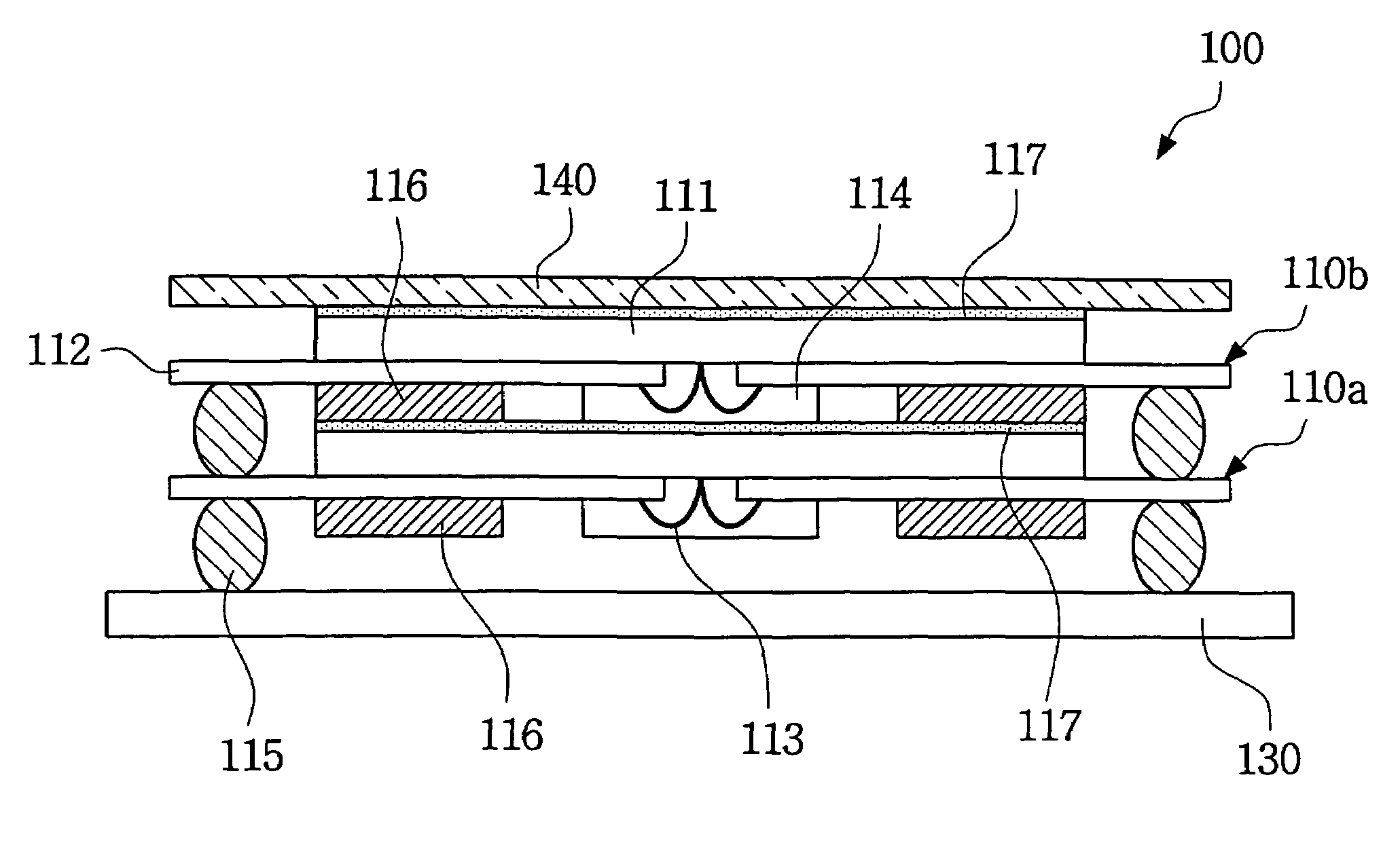
[0036]A cross-section of a stack package in accordance with a first exemplary embodiment of the present invention is shown in FIG. 6. The stack package 100, shown in FIG. 6, has a two-layered structure in which two individual packages 110a and 110b are arranged in layers. A lower individual package 110a has the same configuration as an upper individual package 110b. A cross-section of each individual package is shown in FIG. 7A. Furthermore, FIGS. 7B and 7C show, in plan views, bottom and top configurations of the individual package shown in FIG. 7A.
[0037]Referring to FIGS. 6, 7A, 7B and 7C, each individual package 110 includes an integrated circuit (IC) chip 111 that is attached to a circuit substrate 112. The circuit substrate 112 has a top face 112b to which the IC chip 111 is attached, and a bottom face 112a opposite the top face 112b. The circuit substrate 112 also has a central opening that extends lengthwise. The IC chip 111 has chip pads (not shown) that are formed on an act...
second exemplary embodiment
[0045]A cross-section of a stack package in accordance with a second exemplary embodiment of the present invention is shown in FIG. 8. The stack package 200, shown in FIG. 8, has a four-layered structure in which four individual packages 210a, 210b, 210c and 210d are arranged in layers. Each individual package 210a, 210b, 210c and 210d has the same configuration as described in the foregoing embodiment.
[0046]The stack package 200 particularly includes a plurality of dummy balls 250 that are provided between the lowermost individual package 210a and the module board 130. FIG. 9 shows, in a plan view, a bottom configuration of the lowermost individual package 210a.
[0047]Referring to FIGS. 8 and 9, the dummy balls 250 are formed in rows at the heat-conducting layer 116 on the bottom face of the circuit substrate 112, creating additional heat-dissipating paths from the lowermost individual package 210a to the module board 130. Thus, the heat dissipation of the stack package 200 can be ...
third exemplary embodiment
[0048]A cross-section of a stack package in accordance with a third exemplary embodiment of the present invention is shown in FIG. 10. The stack package 300, shown in FIG. 10, has a two-layered structure in which two individual packages 310 and 320 are arranged in layers. Unlike the foregoing embodiments, the upper and lower individual packages 310 and 320 are slightly different from each other in configuration.
[0049]Referring to FIG. 10, the upper individual package 310 has a configuration that the active surface of the IC chip 111 is attached to the top face of the circuit substrate 112, whereas the lower individual package 320 has an opposite configuration with the active surface of the IC chip 111 attached to the bottom face of the circuit substrate 112. All the solder balls 115 of both individual packages 310 and 320 are still provided on the bottom face of the respective circuit substrates 112.
[0050]Particularly, each of the IC chips 111 faces the outside of the stack package ...
PUM
 Abstract
Description
Claims
Application Information