Duobinary optical transmission device using at least one semiconductor optical amplifier

a transmission device and semiconductor technology, applied in the direction of electromagnetic transmission, transmission, semiconductor amplifier structure, etc., can solve the problems of limited transmission distance, interference and distortion, limited transmission capacity extension in optical systems, etc., to improve the non-linearity and dispersion characteristics of non-return-to-zero, and improve transmission. the effect of non-return to zero

Inactive Publication Date: 2009-01-06
SAMSUNG ELECTRONICS CO LTD
View PDF19 Cites 29 Cited by
  • Summary
  • Abstract
  • Description
  • Claims
  • Application Information

AI Technical Summary

Benefits of technology

[0015]Therefore, the present invention provides a duobinary optical transmission device using at least one semiconductor optical amplifier whose output does not have its transmission quality and bit pattern dependent upon the filter transmission characteristics of the filter used, as in the conventional duobinary optical transmitter. In addition, the present invention provides an improvement in transmission, particularly with regard to improve non-linearity and dispersion characteristics of non-return-to-zero (NRZ) transmission.

Problems solved by technology

However, the extension of transmission capacity in an optical system is limited due to interference and distortion between channels at a channel interval of 50 GHz or less at the time of performing optical intensity modulation using existing non-return-to-zero (NRZ) protocol.
The interference and distortion is related both to increased data traffic and high-speed data transmission demands of 40 Gbps or more.
When a direct current (DC) frequency component of an existing binary NRZ transmission signal and a high-frequency component transmitted by spread spectrum modulation are propagated in an optical fiber medium, problems associated with non-linearity and dispersion are sufficient so as to limit the transmission distance is limited in a high-speed transmission of 10 Gbps or more.
As the length of the PRBS increases, transmission characteristics are further degraded, such that it is difficult for the system to be implemented.
However, there is a structural problem in that a shift from the “0” level to the “1” level, or a shift from the “1” level to the “0” level occurs and hence the jitter of an output waveform increases, because parts having differing slopes are combined in case of a duobinary optical transmitter using the electrical LPF.
This problem occurs in the conventional Z-cut or X-cut structure.
The dependence of this signal pattern causes the system margin to be limited when optical transmission is performed.
However, there are problems in this conventional technique in that an expensive phase modulator must be used, which does not permit implementation of a cost-effective transmission device.

Method used


Image

  • Duobinary optical transmission device using at least one semiconductor optical amplifier
  • Duobinary optical transmission device using at least one semiconductor optical amplifier
  • Duobinary optical transmission device using at least one semiconductor optical amplifier

Examples


Embodiment Construction

[0027]Now, several aspects and advantages of the present invention will be described in detail with reference to the annexed drawings. In the drawings, the same or similar elements are denoted by the same reference numerals even though they are depicted in different drawings. In the following description, a detailed description of known functions and configurations incorporated herein will be omitted when it may make obscure the subject matter of the present invention.

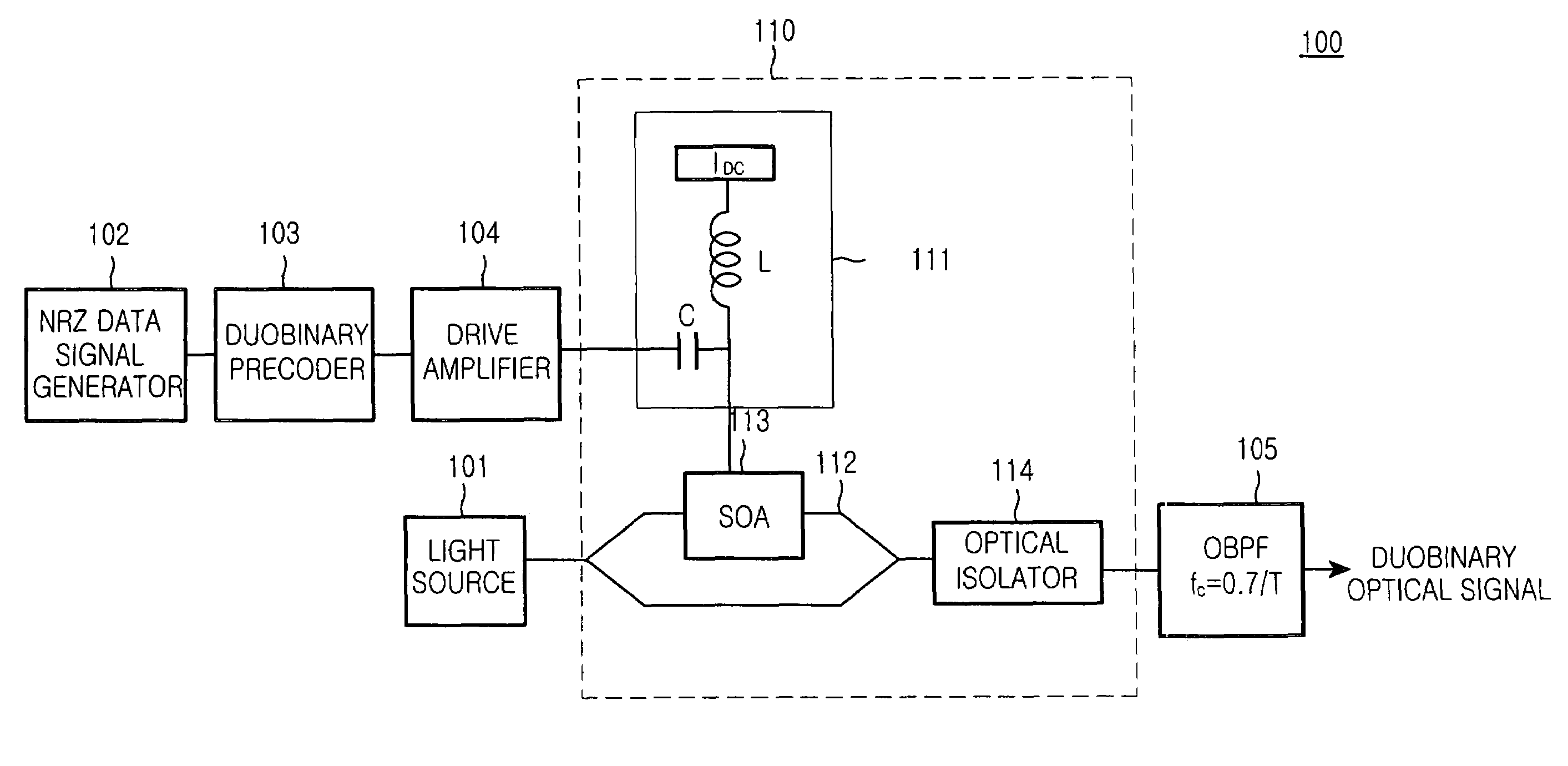
[0028]FIG. 4 is a block diagram illustrating the configuration of a duobinary optical transmission device 100 using a semiconductor optical amplifier (SOA) in accordance with a first aspect of the present invention.

[0029]Referring to FIG. 4, one example of the duobinary optical transmission device 100 of the present invention includes a light source 101 for outputting a carrier wave; a signal generator 102 for generating a non-return-to-zero (NRZ) data or electrical signal; a duobinary precoder 103 for encoding the NRZ...


PUM


Abstract

A duobinary optical transmission device provides duobinary optical transmission with improved quality by a technique that does not require an electrical low pass filter LPF.A duobinary optical transmission device includes at least one semiconductor optical amplifier (SOA). A light source outputs a carrier wave as an optical signal. A precoder encodes an input of a non-return-to-zero (NRZ) electrical signal. An interferometer type semiconductor optical amplification unit modulates the carrier wave according to a change of an applied bias current coupled to the encoded signal. An optical band pass filter (OBPF) receives the phase-modulated optical signal from the semiconductor optical amplification unit, filters the received phase-modulated optical signal according to a designated band, and outputs an optical duobinary signal.

Description

CLAIM OF PRIORITY[0001]This application claims priority to an application entitled “DUOBINARY OPTICAL TRANSMISSION DEVICE USING AT LEAST ONE SEMICONDUCTOR OPTICAL AMPLIFIER,” filed in the Korean Intellectual Property Office on Aug. 27, 2003 and assigned Serial No. 2003-59537, the contents of which are hereby incorporated by reference.BACKGROUND OF THE INVENTION[0002]1. Field of the Invention[0003]The present invention relates to a duobinary optical transmission device using a duobinary optical transmission technique. More particularly, the present invention relates to a duobinary optical transmission device using at least one semiconductor optical amplifier (SOA).[0004]2. Description of the Related Art[0005]An optical transmission system based on dense wavelength division multiplexing (DWDM) transmits an optical signal comprising a plurality of channels having different wavelengths that are transmitted on a single optical fiber, thereby increasing the transmission efficiency. Due to...

Claims


Application Information

Patent Timeline
Patent Type & Authority Patents(United States)
IPC IPC(8): H04B10/00H01S5/50H04B10/25H04B10/2507H04B10/516H04B10/556H04B10/588H04B10/61
CPCH04B10/505H04B10/5055H04B10/508H04B10/50H04B10/516H04B10/2581
Inventor LEE, HAN-LIMLEE, GYU-WOONGOH, YUN-JEHWANG, SEONG-TAEK
Owner SAMSUNG ELECTRONICS CO LTD
Why Eureka
Try Eureka