Selective formation of metal layers in an integrated circuit

a technology of integrated circuits and metal layers, applied in the direction of coatings, metallic material coating processes, chemical vapor deposition coatings, etc., can solve the problems of increasing the effective k-value of interlevel dielectrics, failure of primary reliability modes, and many process steps, so as to enhance the reliability of copper interconnects

Active Publication Date: 2009-01-13
ASM JAPAN
View PDF19 Cites 110 Cited by
  • Summary
  • Abstract
  • Description
  • Claims
  • Application Information

AI Technical Summary

Benefits of technology

[0013]According to yet another aspect of the invention, a method is provided for enhancing reliability of a copper interconnect. The method comprises providing a copper surface and a dielectric surface. The copper and dielectric surfaces are contacted with a vapor phase compound of a noble metal. A reliability enhancing layer of noble metal is formed on the copper surface selectively relative to the dielectric surface by supplying a vapor phase compound of the noble metal. In one embodiment, the copper surface is exposed at the bottom of vias. In another embodiment, the copper surface is the upper surface of an inlaid copper line and the dielectric surface coplanar with the copper surface.

Problems solved by technology

This would lead to two primary modes of reliability failure.
Additional disadvantage of separate blanket CVD dielectric capping layers is an increase of effective k-value for interlevel dielectrics.
Additionally, adhesion of copper at the via bottom is critical to interconnect reliability because interconnect failure frequently occurs at a via due to migration of copper atoms due to electrical current (EM) or mechanical stress during thermal cycle (stress-induced voiding or SIV).
However, this method has disadvantages, such as many process steps and severe process control and cost issues.

Method used


Image

  • Selective formation of metal layers in an integrated circuit
  • Selective formation of metal layers in an integrated circuit
  • Selective formation of metal layers in an integrated circuit

Examples


Embodiment Construction

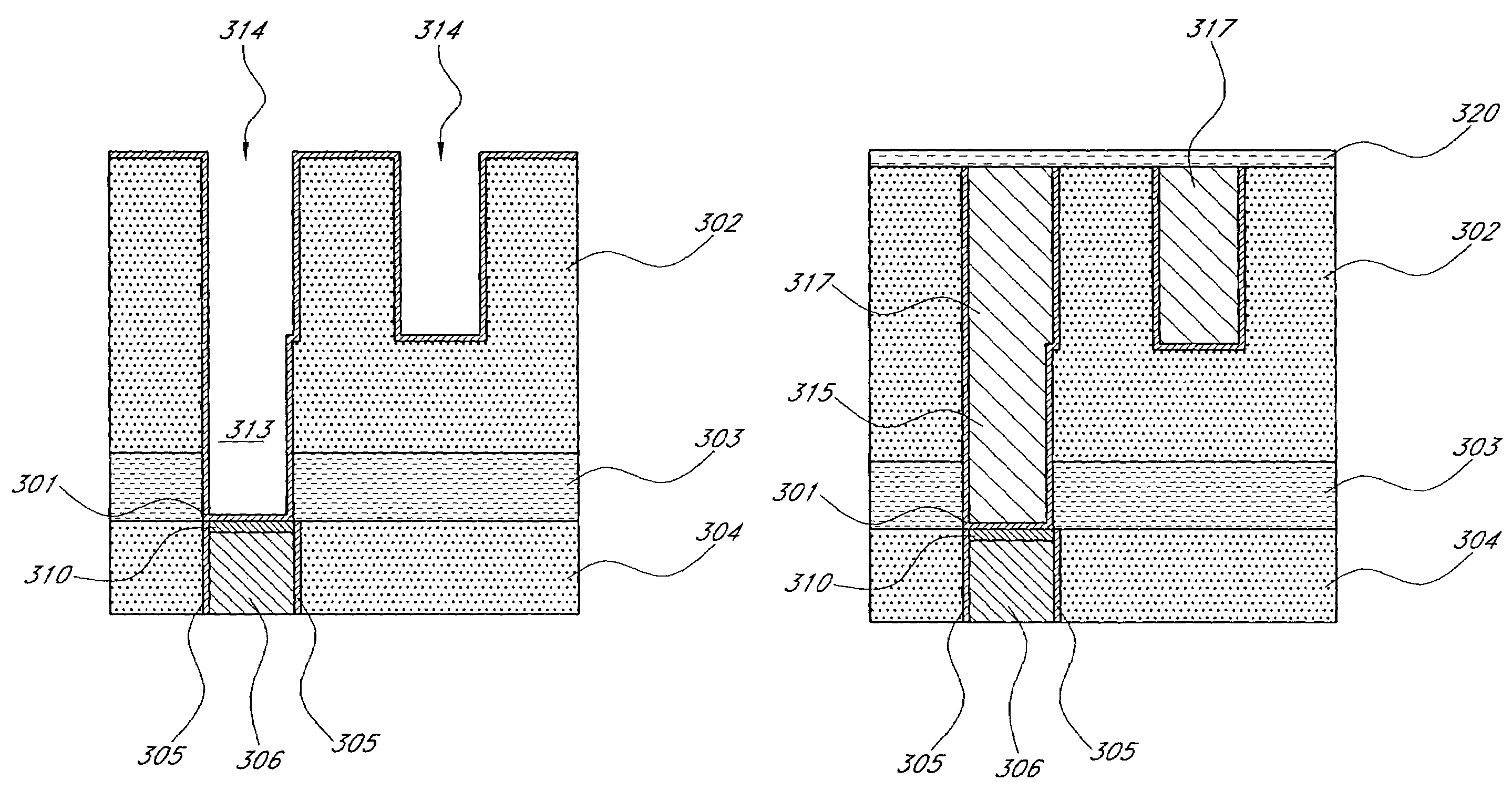
[0024]Reliability enhancing material can be selectively formed only on exposed interconnect (e.g, copper) surfaces at, for example, a via bottom and / or the exposed upper surface of a copper interconnect, forming metal capping layers. One method is by exploiting faster nucleation on a metal surface relative to an insulating surface, thereby depositing noble metal atoms (e.g., by selective CVD or ALD) on the metal surface. Another method is by replacing copper atoms on an exposed copper layer with noble metal atoms using a replacement reaction. Additional noble metal atoms may be deposited (e.g., by selective CVD or ALD) on the Cu-replacing noble metal layer to increase the thickness of a reliability-enhancing layer. Advantageously, the methods of illustrated embodiments employ vapor phase reactants.

[0025]After patterning and etching, the surface of a damascene or dual damascene structure comprises mainly dielectric materials: low-k material, dielectric barrier layer and additional ma...


PUM

PropertyMeasurementUnit
temperatureaaaaaaaaaa
pressureaaaaaaaaaa

Abstract

A method for enhancing the reliability of copper interconnects and / or contacts, such as the bottom of vias exposing top surfaces of buried copper, or at the top of copper lines just after CMP. The method comprises contacting the exposed copper surface with a vapor phase compound of a noble metal and selectively forming a layer of the noble metal on the exposed copper surface, either by a copper replacement reaction or selective deposition (e.g., ALD or CVD) of the noble metal.

Description

[0001]This application claims the priority benefit under 35 U.S.C. § 119(e): U.S. patent application Ser. No. 60 / 622,141 to Kilpera, filed Oct. 26, 2004; and U.S. patent application Ser. No. 60 / 662,144 to Huotari et al., filed Mar. 15, 2005.BACKGROUND OF THE INVENTION[0002]1. Field of the Invention[0003]The present invention generally relates to a method of selectively forming metal layers, more specifically to a method of selectively forming noble metal layers.[0004]2. Description of the Related Art[0005]A back-end-of-line (BEOL) copper interconnect is formed by a damascene or dual damascene process. A damascene process involves creating interconnect lines by first etching trenches or vias in a planar dielectric layer and then filling the trench or vias with a metal, typically copper. In a dual damascene process, which is a conventional semiconductor metallization process, another level is involved, where a series of holes (i.e. contact holes or vias) are etched and filled simultan...

Claims


Application Information

Patent Timeline
Patent Type & Authority Patents(United States)
IPC IPC(8): H01L21/44
CPCC23C16/18C23C16/45525H01L21/28562H01L21/32051H01L21/76814H01L21/76834H01L21/76843H01L21/76849
Inventor KILPELA, OLLI V.KOH, WONYONGHUOTARI, HANNU A.TUOMINEN, MARKOLEINIKKA, MIIKA
Owner ASM JAPAN
Why Eureka
Try Eureka