Photodiode array and method for establishing a link between a first semiconductor element and a second semiconductor element

a technology of semiconductor elements and arrays, applied in the direction of lasers, semiconductor lasers, radiation controlled devices, etc., can solve the problems of difficult handling of small singulated chips, time-consuming method, disadvantageous singulated component positioning, etc., and achieve economic and effective effects

Inactive Publication Date: 2009-01-13
OSRAM OPTO SEMICONDUCTORS GMBH
View PDF12 Cites 4 Cited by
  • Summary
  • Abstract
  • Description
  • Claims
  • Application Information

AI Technical Summary

Benefits of technology

[0012]Therefore, the present invention is based on an aspect of providing a photodiode arrangement and a method for producing a connection between a first semiconductor component ...

Problems solved by technology

In this method, the fact that one component has to be positioned in a workpiece carrier after singulation is disadvantageous.
The method is time-consuming and the small size of the singula...

Method used


Image

  • Photodiode array and method for establishing a link between a first semiconductor element and a second semiconductor element
  • Photodiode array and method for establishing a link between a first semiconductor element and a second semiconductor element
  • Photodiode array and method for establishing a link between a first semiconductor element and a second semiconductor element

Examples


Embodiment Construction

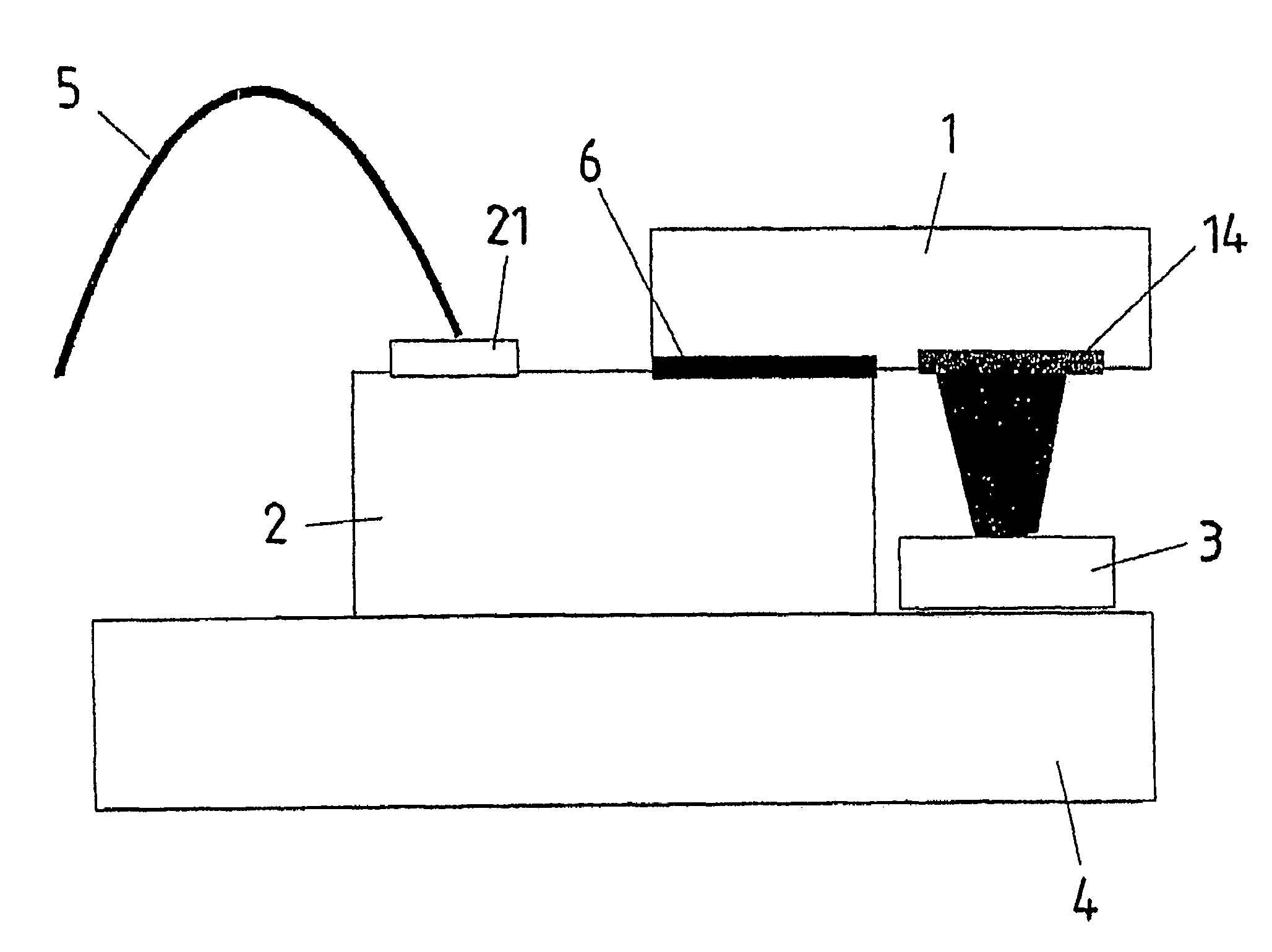
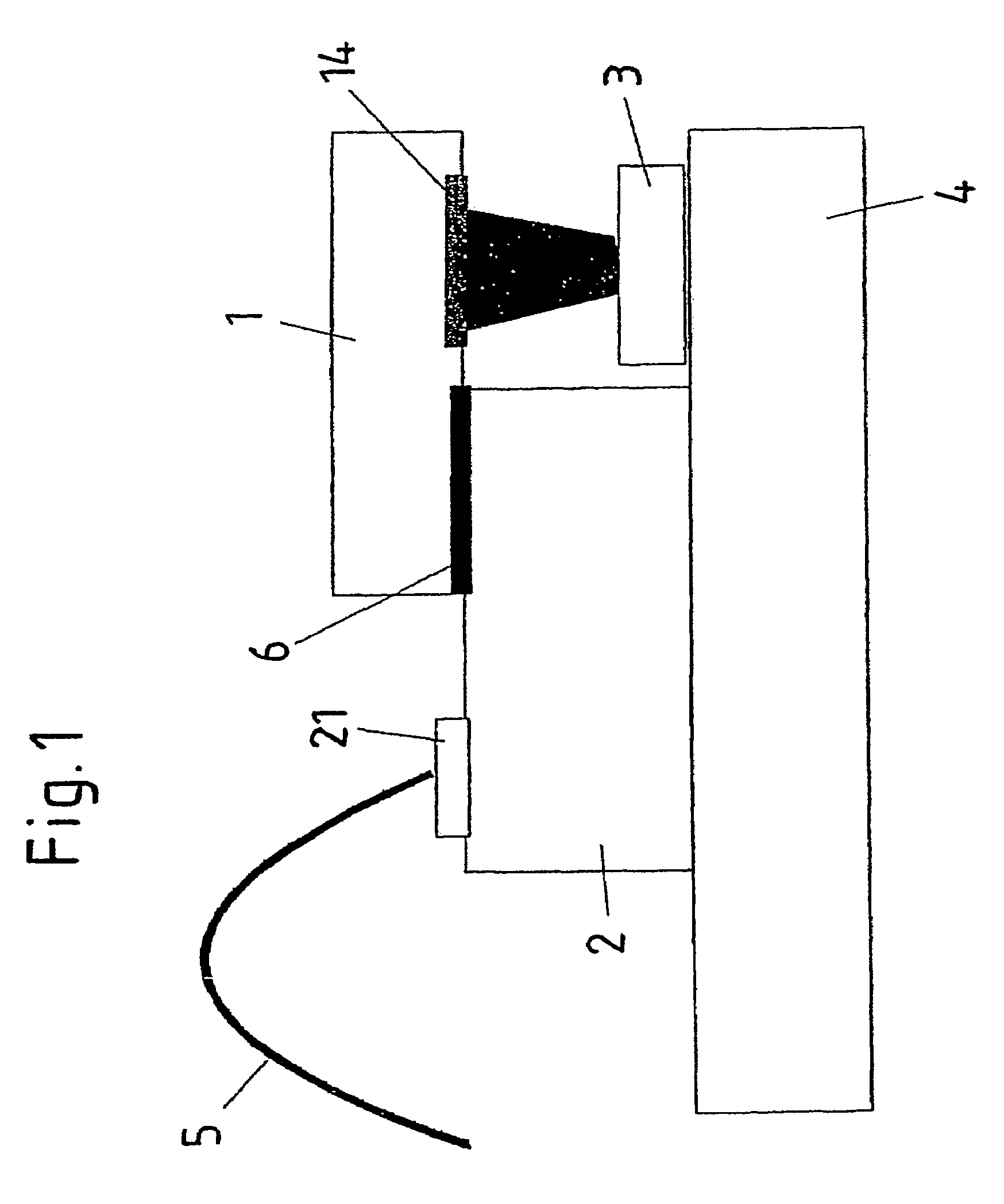
[0041]FIG. 1 shows a photodiode arrangement in which a monitor diode 1 is arranged on a spacer 2. Both the spacer 2 and an array 3 of vertically emitting semiconductor lasers (VCSEL) are positioned on a common carrier 4 in such a way that light emitted by a lateral semiconductor laser of the array is detected directly by the monitor diode 1, the downwardly oriented optically active layer 14 of which projects over the spacer 2.

[0042]The monitor diode 1 is preferably a silicon photodiode. The submount 2 is likewise preferably a silicon chip. The two components 1, 2 in each case have metallizations. In this case, the metallizations of the spacer 2 can each be connected to a bonding wire via a contact pad 21. The two components 1, 2 are connected by means of eutectic bonding whilst still in the wafer composite, as a result of which the monitor diode 1 and the submount 2 are electrically and also mechanically connected to one another in a region 6. This is explained in more detail below ...


PUM


Abstract

The invention relates to a photodiode array comprising a photodiode and a submount, via which the photodiode is contacted, said photodiode and said submount being interlinked by eutectic bonding. The invention further relates to a method for establishing a link between a first semiconductor element and a second semiconductor element which have different outer contours, the two elements being interlinked by eutectic bonding when already being present as a wafer composite. The two interlinked wafers are subdivided one by one and independently of each other in accordance with the desired outer contour.

Description

RELATED APPLICATION[0001]This application is a national stage application of International Application No. PCT / DE02 / 00067 filed Jan. 9, 2002, which is entitled “PHOTODIODE ARRAY AND METHOD FOR ESTABLISHING A LINK BETWEEN A FIRST SEMICONDUCTOR ELEMENT AND A SECOND SEMICONDUCTOR ELEMENT”, which was not published in English, which is hereby incorporated by reference in its entirety.FIELD OF THE INVENTION[0002]The invention relates to a photodiode arrangement having a photodiode and a submount, via which the photodiode is electrically contact-connected, and a method for producing a connection between a first semiconductor component and a second semiconductor component, in particular between a photodiode and a submount for a photodiode, the semiconductor components connected to one another having a different outer contour.BACKGROUND OF THE INVENTION[0003]DE 197 09 842 C1 discloses an electro-optical coupling assembly with a laser diode arrangement in which a plurality of vertically emitt...

Claims


Application Information

Patent Timeline
IPC IPC(8): H01L31/12H01L27/146H01L31/02H01L31/101H01L31/18H01S5/022
CPCH01L31/02005H01L31/02019H01L31/101H01L31/18H01S5/02248H01L27/14643H01S5/0683H01S5/423H01L2224/48091H01L2924/00014H01S5/02325
Inventor FURST, ROBERTKAMPF, MATHIASRING, MELANIESINGER, FRANK
Owner OSRAM OPTO SEMICONDUCTORS GMBH
Why Eureka
Try Eureka