DLL circuit feeding back ZQ calibration result, and semiconductor device incorporating the same

a dll circuit and zq technology, applied in the field of semiconductor devices, can solve the problems of dll circuits that cannot achieve high-speed operation, unable to achieve temperature, voltage measurement variations, and difficulty in performing control that can absorb variations, so as to reduce a skew of dq output timing

Active Publication Date: 2009-01-13
LONGITUDE LICENSING LTD
View PDF8 Cites 23 Cited by
  • Summary
  • Abstract
  • Description
  • Claims
  • Application Information

AI Technical Summary

Benefits of technology

[0014]It is therefore an object of this invention to provide a DLL circuit that reduces a skew by feeding back a ZQ calibration result to the DLL circuit.
[0017]A DDR3-SDRAM has a ZQ calibration function of measuring an external resistance element connected to a dedicated pad. This external resistance element is not subjected to a change caused by variations in temperature, voltage, and process. Therefore, the result of this ZQ calibration is a result reflecting variations in temperature, voltage, and process and thus can compensate for a change caused by these variations. Using this ZQ calibration result as control data, a delay amount of a replica system path of a DLL circuit is adjusted. It becomes possible to reduce a skew of the output timing by feeding back the ZQ calibration result to the DLL circuit. With this configuration, it becomes possible to provide the DLL circuit with a reduced skew and the semiconductor device having such a DLL circuit.
[0030]The foregoing DLL circuits each adjust a delay amount of the replica system path of the DLL circuit on the basis of a ZQ calibration result obtained by an external resistance element connected to a ZQ calibration dedicated pad. This external resistance element is not subjected to a change caused by variations in temperature, voltage, and process. Therefore, this ZQ calibration result can be used as data for compensating for variations in temperature, voltage, and process in the semiconductor device. It becomes possible to reduce a skew of the output timing by feeding back the ZQ calibration result to the DLL circuit.
[0032](1) It is possible to reduce a skew of the DQ output timing caused by a difference in circuit structure between a DQ replica and a DQ buffer.
[0033](2) It is possible to reduce a skew of the DQ output timing caused by variations in temperature, voltage, and process.

Problems solved by technology

Therefore, it is difficult to perform control that can absorb those variations.
That is, there has been a problem that variations in delay amount of the DQ buffer system and delay amount of the DQ replica system caused by variations in temperature, voltage, and Vth of MOS transistors become skews as they are and thus the DLL circuit cannot achieve high-speed operation.
However, in the conventional DLL circuit, there is no function of measuring variations in temperature, voltage, and Vth of MOS transistors and feeding them back.
Therefore, there remains the problem that variations in delay amount of the output system and delay amount of the replica system caused by variations in temperature, voltage, and Vth of MOS transistors become skews as they are and thus the high-speed operation cannot be achieved.
Further, also in the conventional calibration circuits and memory system, no improvement scheme for these skews is proposed and thus there still remains the problem.
Therefore, there is the problem that variations in delay amount of the DQ buffer system path and delay amount of the DQ replica system path caused by variations in temperature, voltage, and Vth of MOS transistors become skews as they are and thus the high-speed operation cannot be achieved.

Method used


Image

  • DLL circuit feeding back ZQ calibration result, and semiconductor device incorporating the same
  • DLL circuit feeding back ZQ calibration result, and semiconductor device incorporating the same
  • DLL circuit feeding back ZQ calibration result, and semiconductor device incorporating the same

Examples


Embodiment Construction

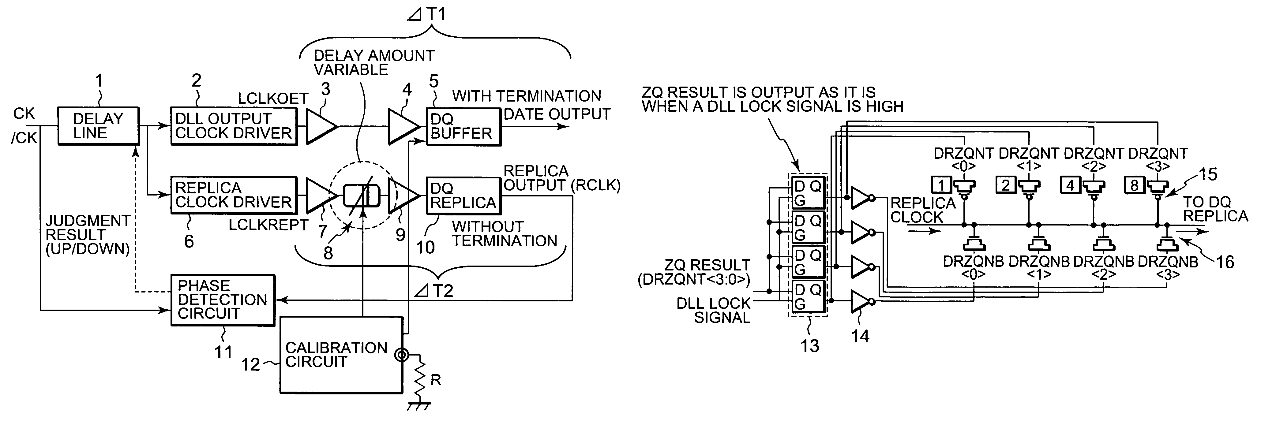
[0042]At first, referring to FIG. 3A, description will be made of a DLL circuit according to an embodiment of this invention.

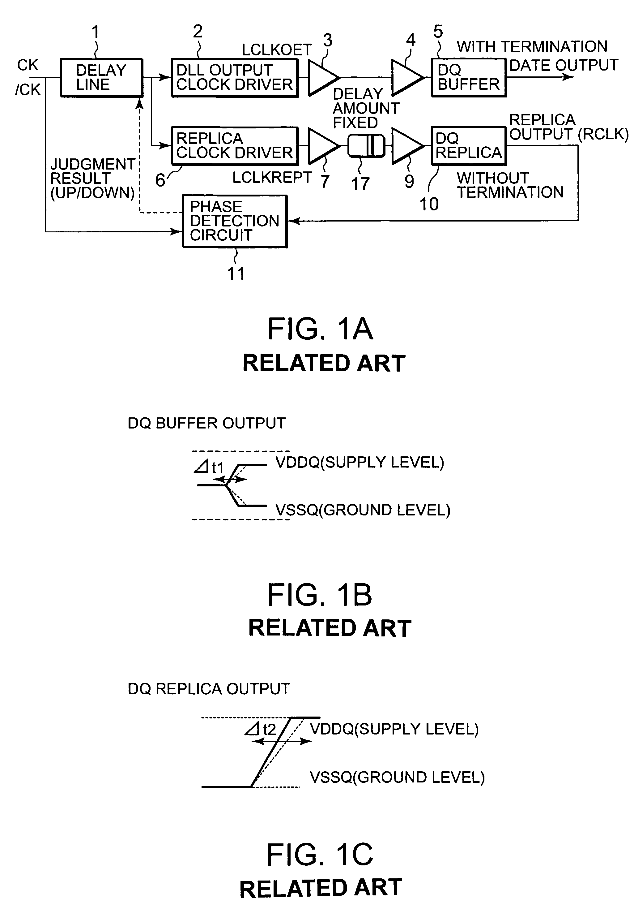
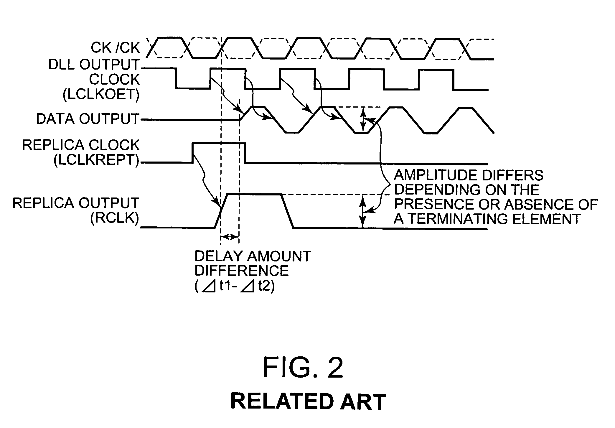
[0043]Clocks (CK, / CK) input from the exterior are propagated to the DLL circuit through a DLL circuit-dedicated initial input stage. The properly delayed clock having passed through a delay line 1 is sent, through a DLL output clock driver 2 and buffers 3 and 4, to a DQ buffer 5 that performs memory data output. The path from the DLL output clock driver 2 to the DQ buffer 5 will be called a DQ buffer system path.

[0044]On the other hand, the clock having passed through the delay line 1 is also sent, through a replica clock driver 6, a buffer 7, a delay amount variable circuit 8, and a buffer 9, to a DQ replica 10 that simulates the same operation as that of the DQ buffer 5. The path from the replica clock driver 6 to the DQ replica 10 will be called a DQ replica system path. A phase detection circuit 11 monitors an output of the DQ replica 10 instead of an out...


PUM


Abstract

A delay amount variable circuit (8) adapted to change a delay amount according to a ZQ calibration result is inserted in a path of a DQ replica system. The delay amount of the path of the DQ replica system is variable and is adjusted so as to make constant a timing skew difference between a DQ buffer system and the DQ replica system. The ZQ calibration result changes depending on variations in temperature, voltage, and manufacture. Therefore, by obtaining the delay amount corresponding to these variations, there are obtained a DLL circuit with high accuracy that can make the skew difference constant, and a semiconductor device incorporating such a DLL circuit.

Description

[0001]This application claims priority to prior application JP 2005-308072, the disclosure of which is incorporated herein by reference.BACKGROUND OF THE INVENTION[0002]1. Field of the Invention[0003]This invention relates to a semiconductor device and, in particular, relates to a DLL (Delay Locked Loop) circuit using a result of ZQ calibration adapted for adjusting the impedance of an output circuit and to a semiconductor device incorporating such a DLL circuit.[0004]2. Description of the Related Art[0005]Recent electronic systems have been speeded up in operation, wherein the data transfer rate between semiconductor devices forming the system has been highly increased. Further, also in each of the semiconductor devices, high-speed data transfer operation is required. Accordingly, a clock synchronization system synchronous with a clock signal (hereinafter also referred to simply as a “clock”) is employed inside the semiconductor device. For example, there is a synchronous dynamic r...

Claims


Application Information

Patent Timeline
Patent Type & Authority Patents(United States)
IPC IPC(8): H03L7/00G06F1/10G11C11/401G11C11/407G11C11/4076G11C11/4093H03K5/135H03L7/081
CPCG11C7/1051G11C7/1066G11C7/22G11C7/222H03K5/131H03L7/0812H03L7/0816
Inventor FUJISAWA, HIROKITAKISHITA, RYUJI
Owner LONGITUDE LICENSING LTD
Why Eureka
Try Eureka