Variable impedance sense architecture and method

Active Publication Date: 2009-01-20
MONTEREY RES LLC
View PDF9 Cites 18 Cited by
  • Summary
  • Abstract
  • Description
  • Claims
  • Application Information

AI Technical Summary

Problems solved by technology

The accuracy of impedance sense and matching circuit can be limited by the architecture and various error sources.
However, while one set of calibration codes can provide an initial impedance match for I/Os of a device, operating conditions can result in changes (i.e., drift) in circuit components.
A chattering of an LSB bit can cause significant noise in a driver circuit and adversely affect its performance.
First, an input offset voltage can be a significant source of error in the VIS circuit 1300. An input offset voltage can arise from numerous sources, including but not limited to an input offset at the inputs of comparator 1308, an error in reference voltage Vref, and/or an overdrive voltage of the comparator 1308. Thus, as the accuracy requirements for impedance matching become more precise, the error induced due to such an input offset can result in an unacceptably inaccurate response. Still further, the effect of a comparator input offset on overall matching accuracy can increase as the operating supply voltage decreases. As a result, at such lower power supply levels, an o

Method used


Image

  • Variable impedance sense architecture and method
  • Variable impedance sense architecture and method
  • Variable impedance sense architecture and method

Examples


Embodiment Construction

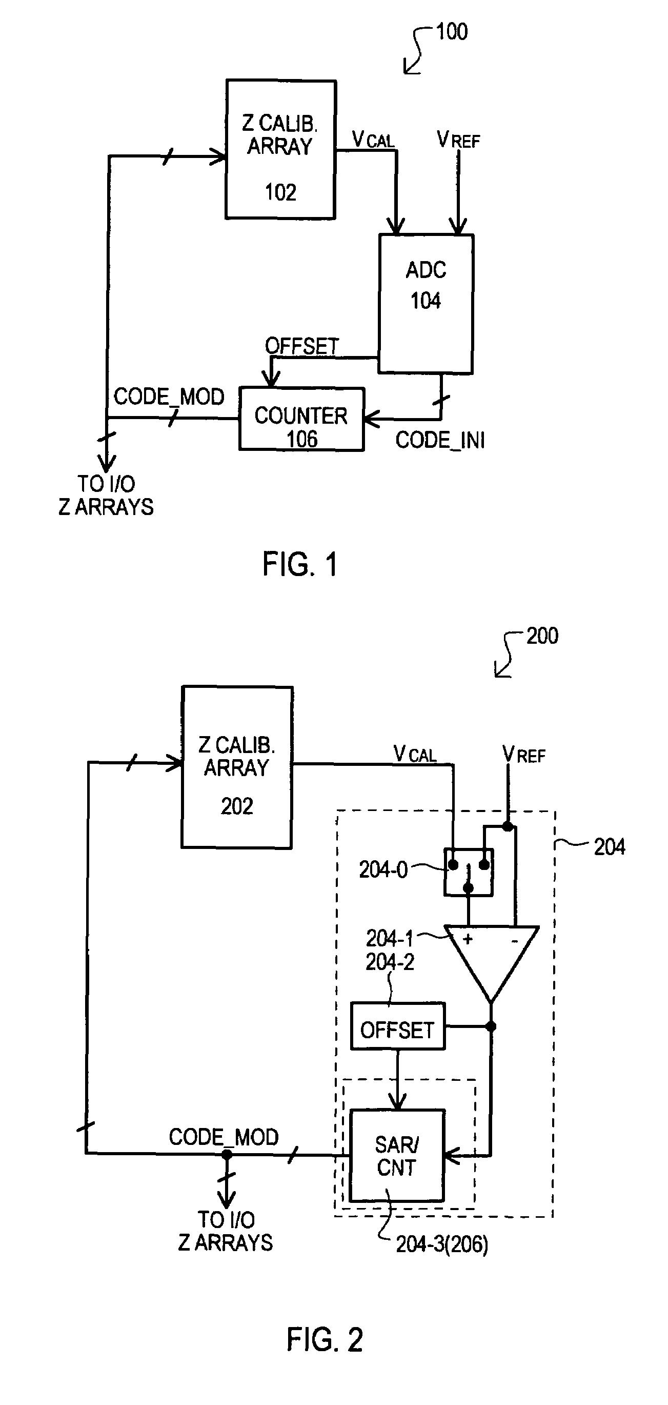
[0060]The various embodiments of the present invention are directed to variable impedance sense (VIS) circuits and methods. The disclosed embodiments can compensate for errors arising from offset voltages inherent in the sensing circuitry.

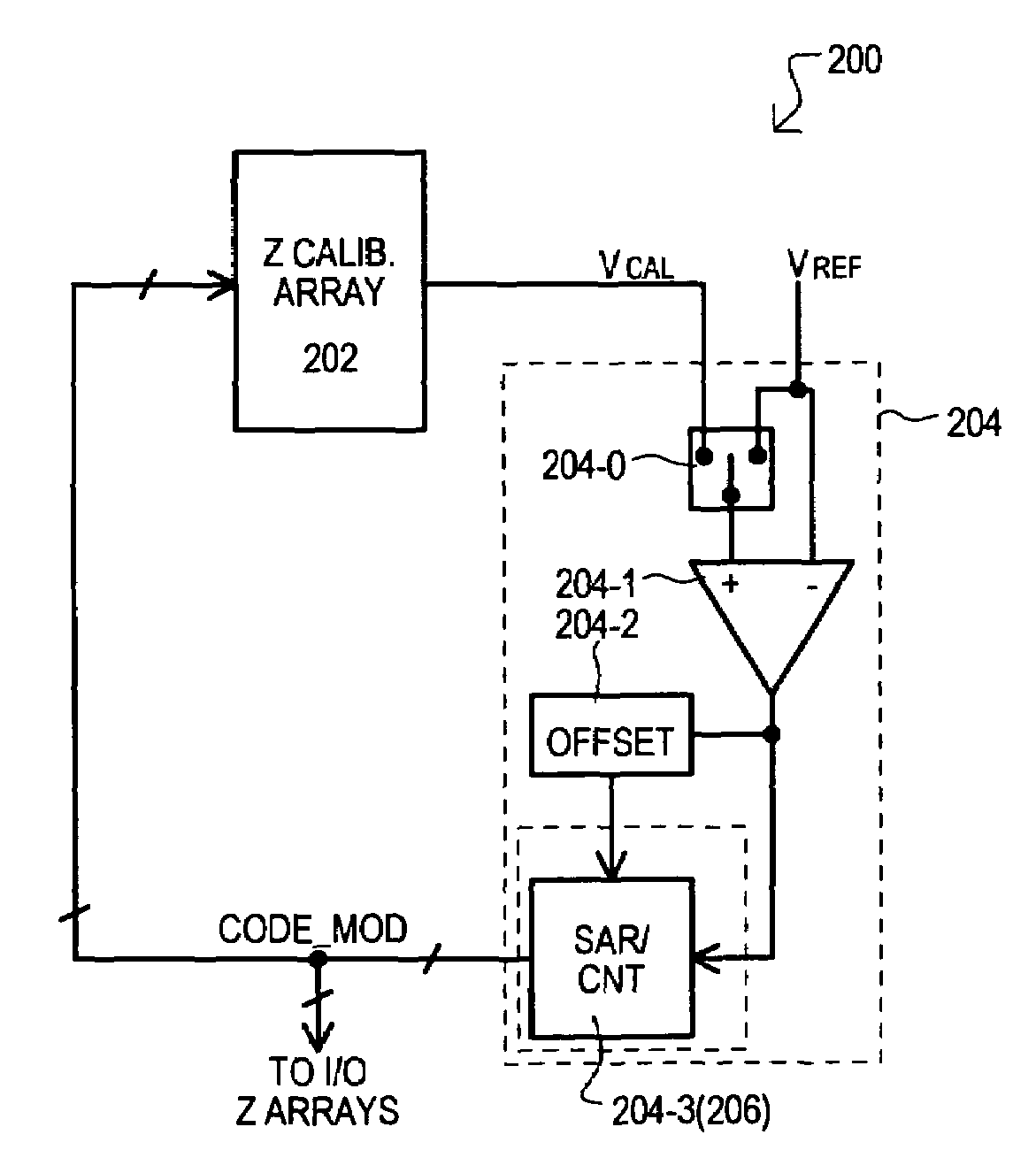
[0061]Referring now to FIG. 1, a VIS circuit 100 according to a first embodiment is shown in a block schematic diagram. A VIS circuit 100 can include a calibration impedance array 102, an analog-to-digital converter (ADC) circuit 104, and a counter circuit 106. An impedance (Z) calibration array 102 can provide a variable impedance based on a received input code CODE_MOD. An ADC circuit 104 can receive a calibration voltage (VCAL) from Z calibration array 102 and a reference voltage (VREF). ADC circuit 104 can generate an initial digital code value CODE_INI corresponding to a received calibration voltage (VCAL). Initial code value CODE_INI can be provided to a counter circuit 106.

[0062]Unlike a conventional arrangement like that of FIG. 13, an ADC ...


PUM


Abstract

A variable impedance sense (VIS) circuit (600) can detect and store an input offset value inherent in a sensing loop (620 and/or 622). According to a detected input offset polarity, a resulting impedance matching binary code can be adjusted to compensate for error that can be introduced by the input offset. The binary code can also be adjusted to compensate for additional error that can be introduced by dropping a least significant bit (LSB) of the code to reduce noise effects caused by the switching of the LSB.

Description

[0001]This application claims the benefit of U.S. provisional patent application Ser. No. 60 / 722,612 filed on Sep. 29, 2005, the contents of which are incorporated by reference herein.TECHNICAL FIELD[0002]The present invention relates generally to input / output (I / O) circuits, and more particularly to I / O circuits that can provide impedance matching by sensing a reference impedance value.BACKGROUND OF THE INVENTION[0003]Integrated circuits and other electronic devices can include input and / or output (I / O) connections for transmitting and receiving signals. As signal transmission speeds have increased, impedance matching has become an increasingly important feature in such devices. Matching impedance with external package and / or circuit board traces can improve the signal integrity and performance of both a signal transmitter and receiver.[0004]In order to match signal line impedance, I / O circuits can include variable impedance circuits that can be adjusted as needed to match a sensed...

Claims


Application Information

Patent Timeline
IPC IPC(8): H03K17/16H03K19/003
CPCH03K19/0005H03K19/00369
Inventor VULLAGANTI, KALYANA C.HUNT, JEFFERY SCOTT
Owner MONTEREY RES LLC
Why Eureka
Try Eureka