Substrate processing method

a processing method and substrate technology, applied in the direction of basic electric elements, semiconductor/solid-state device manufacturing, electric devices, etc., can solve the problems of difficult removal, delay in operation speed, and lower signal propagation ra

Inactive Publication Date: 2009-01-27
TOKYO ELECTRON LTD
View PDF10 Cites 15 Cited by
  • Summary
  • Abstract
  • Description
  • Claims
  • Application Information

AI Technical Summary

Benefits of technology

[0012]An object of the present invention is to provide a substrate processing method such that, where a process for removing a residual substance of, e.g., a sacrificial film is performed subsequently to etching of an etching-target film, by solubilizing the residual substance relative to a predetermined liquid, and then removing the residual substance by the predetermined liquid, the method brings about little damage, such as pattern peeling.
[0013]Another object of the present invention is to provide a substrate processing method, which can, in addition to that described above, suppress deterioration in an electric property of an etching-target film due to damage caused by a process for removing a residual substance.
[0023]According to the present invention, etching is performed on an etching target film that can be easily damaged, such as a Low-k film, while using a substance difficult to remove, such as a sacrificial film. Then, a process for removing a residual substance of, e.g., the sacrificial film is performed, by solubilizing the residual substance relative to a predetermined liquid, and then dissolving and removing the residual substance by the predetermined liquid. At this time, a silylation process is performed to recover damage of the etching target film before dissolving and removing the residual substance. Consequently, it is possible to prevent pattern damage, such as pattern CD loss, from being caused by dissolving and removing the residual substance.
[0024]Further, where additional silylation process is performed after dissolving and removing the residual substance, it is possible to recover a deterioration in the electric property of the etching-target film due to damage caused by dissolving and removing the residual substance.

Problems solved by technology

In semiconductor devices, a decrease in the interconnection line space due to miniaturization increases the capacitance between interconnection lines, which makes the signal propagation rate lower, thereby resulting in a delay in operation speed.
Incidentally, the sacrificial film 207 is sometimes made of an Si—O based inorganic material, which is difficult to remove by an ashing process used for removing the conventional resist film.
There is a case where a chemical liquid is used to dissolve a film of this kind, but the processing rate is very low.
However, when a process is performed by a process gas containing water vapor and ozone, a Low-k material used as an inter-level insulating film having a pattern may be damaged.
The damage in the pattern may become obvious by a subsequent chemical liquid process.
In this case, a Low-k material may be damaged and thereby increase the specific dielectric constant thereof, which deteriorates effects obtained by using the Low-k material as an inter-level insulating film.

Method used


Image

  • Substrate processing method
  • Substrate processing method
  • Substrate processing method

Examples


Embodiment Construction

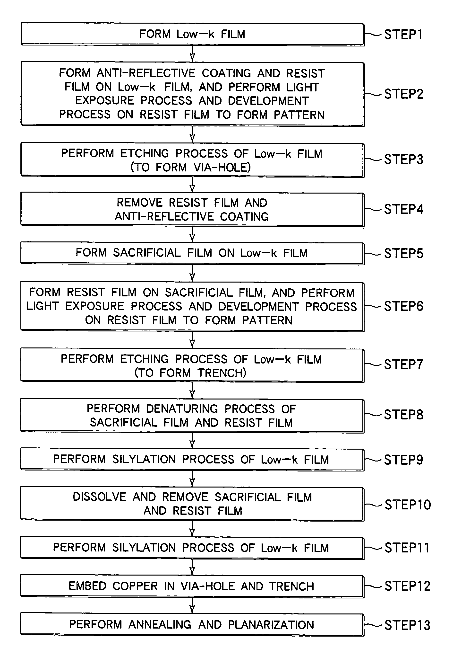
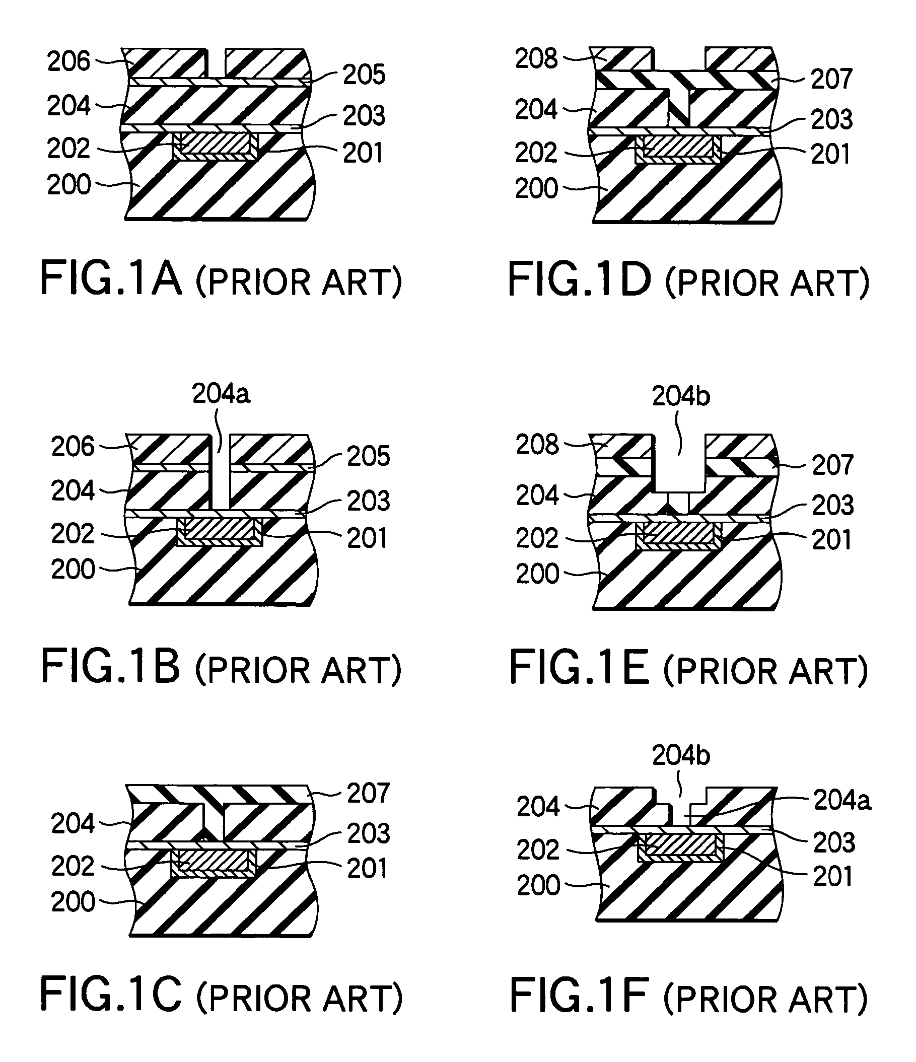
[0036]An embodiment of the present invention will now be described with reference to the accompanying drawings. Hereinafter, the present invention is exemplified by a case where a semiconductor device is manufactured by a dual damascene method.

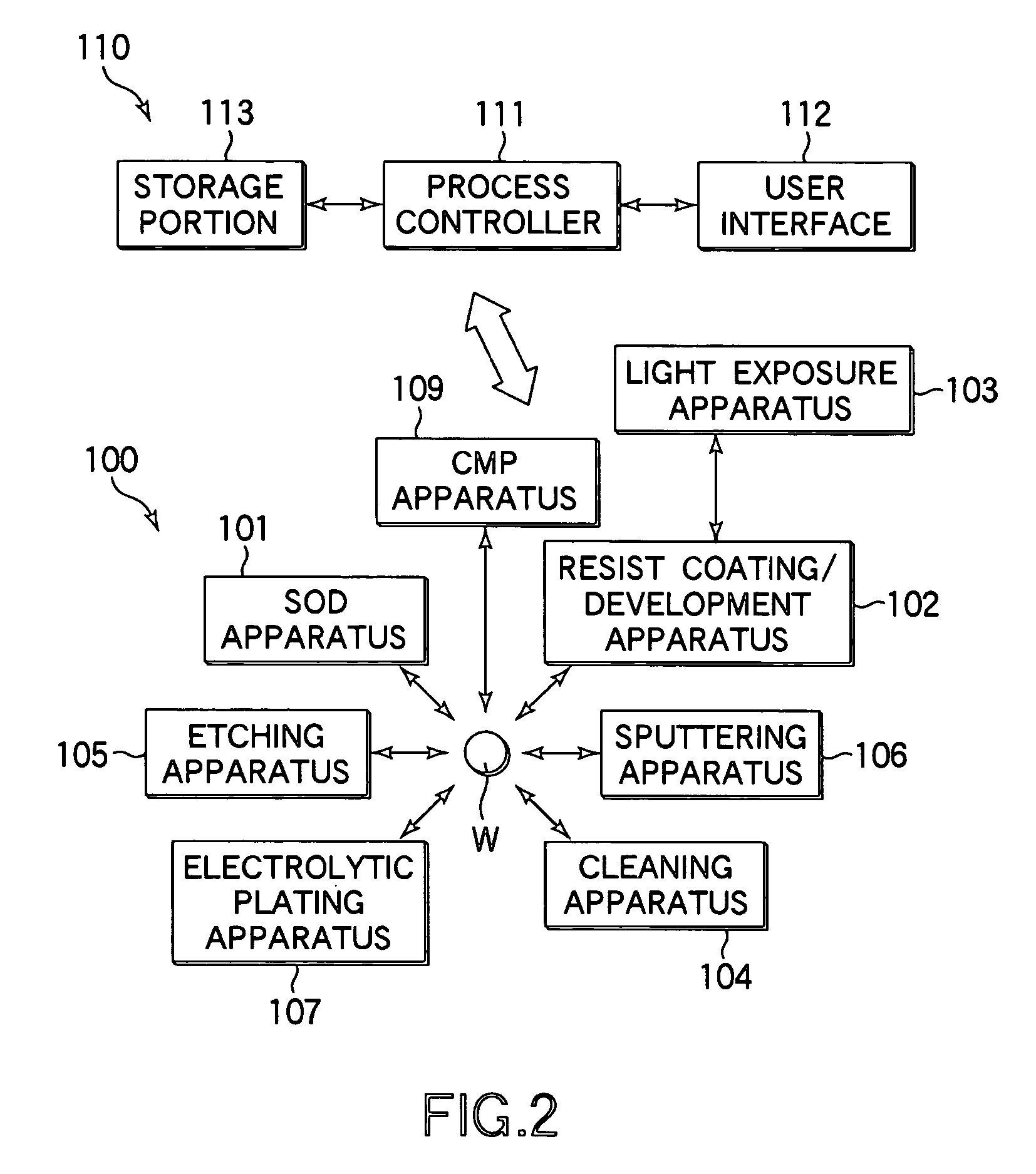
[0037]FIG. 2 is an explanatory view schematically showing the arrangement of a wafer processing system used for a semiconductor device manufacturing process employing a dual damascene method, to which a substrate processing method according to an embodiment of the present invention is applied. This wafer processing system includes a process section 100 and a main control section 110. The process section 100 includes an SOD (Spin On Dielectric) apparatus 101, a resist coating / development apparatus 102, a light exposure apparatus 103, a cleaning apparatus 104, an etching apparatus 105, a sputtering apparatus 106 used as a PVD apparatus, an electrolytic plating apparatus 107, and a CMP apparatus 109 used as a polishing apparatus. The main control...


PUM


Abstract

A substrate processing method includes: performing an etching process to form a predetermined pattern on an etching-target film disposed on a substrate; denaturing a substance remaining after the etching process to be soluble in a predetermined liquid; then, performing a silylation process on a surface of the etching-target film having the pattern formed thereon; and then, supplying the predetermined liquid to dissolve and remove the denatured substance.

Description

BACKGROUND OF THE INVENTION[0001]1. Field of the Invention[0002]The present invention relates to a substrate processing method for performing a denaturing process for denaturing a predetermined substance and a process for dissolving and removing the denatured substance, in manufacturing a semiconductor device by use of, e.g., a dual damascene method. The present invention also relates to a computer readable memory medium that stores a control program for executing a method of this kind.[0003]2. Description of the Related Art[0004]In semiconductor devices, a decrease in the interconnection line space due to miniaturization increases the capacitance between interconnection lines, which makes the signal propagation rate lower, thereby resulting in a delay in operation speed. In order to solve this problem, developments are being made in insulative materials with a low specific dielectric constant (Low-k materials), and multi-layer interconnection lines using such insulative materials. ...

Claims


Application Information

Patent Timeline
Patent Type & Authority Patents(United States)
IPC IPC(8): H01L21/302H01L21/461
CPCH01L21/02063H01L21/3105H01L21/31058H01L21/31111H01L21/31133H01L21/67051H01L21/67178H01L21/67207H01L21/76808H01L21/76814H01L21/76826H01L21/76831H01L21/02126H01L21/306H01L21/3063
Inventor FUJII, YASUSHITOSHIMA, TAKAYUKIORII, TAKEHIKO
Owner TOKYO ELECTRON LTD
Why Eureka
Try Eureka