Vertically aligned mode liquid crystal display

a liquid crystal display and vertical alignment technology, applied in optics, instruments, electrical appliances, etc., can solve the problems of enlarge the black matrix, deteriorate the image quality, and generate the distortion of the signals transmitted via the signal wire, so as to reduce the load of the data wire and improve the image quality

Inactive Publication Date: 2009-01-27
TCL CHINA STAR OPTOELECTRONICS TECH CO LTD
View PDF24 Cites 12 Cited by
  • Summary
  • Abstract
  • Description
  • Claims
  • Application Information

AI Technical Summary

Benefits of technology

[0008]An object of the present invention is to improve image quality by reducing the load of a data wire.
[0009]Another object of the present invention is to reduce the light leakage near a data line by decreasing coupling capacitance between the data line and a reference electrode.

Problems solved by technology

The loads due to such a resistances and capacitances of respective wires generate the distortion of the signals transmitted via the signal wires such as RC delay.
In particular, the capacitive coupling between the data lines and the reference electrode drives the liquid crystal molecules disposed therebetween to cause light leakage near the data line, thereby deteriorating the image quality, and the light leakage, in turn, forces to enlarge the black matrix to reduce the aperture ratio.

Method used


Image

  • Vertically aligned mode liquid crystal display
  • Vertically aligned mode liquid crystal display
  • Vertically aligned mode liquid crystal display

Examples


first embodiment

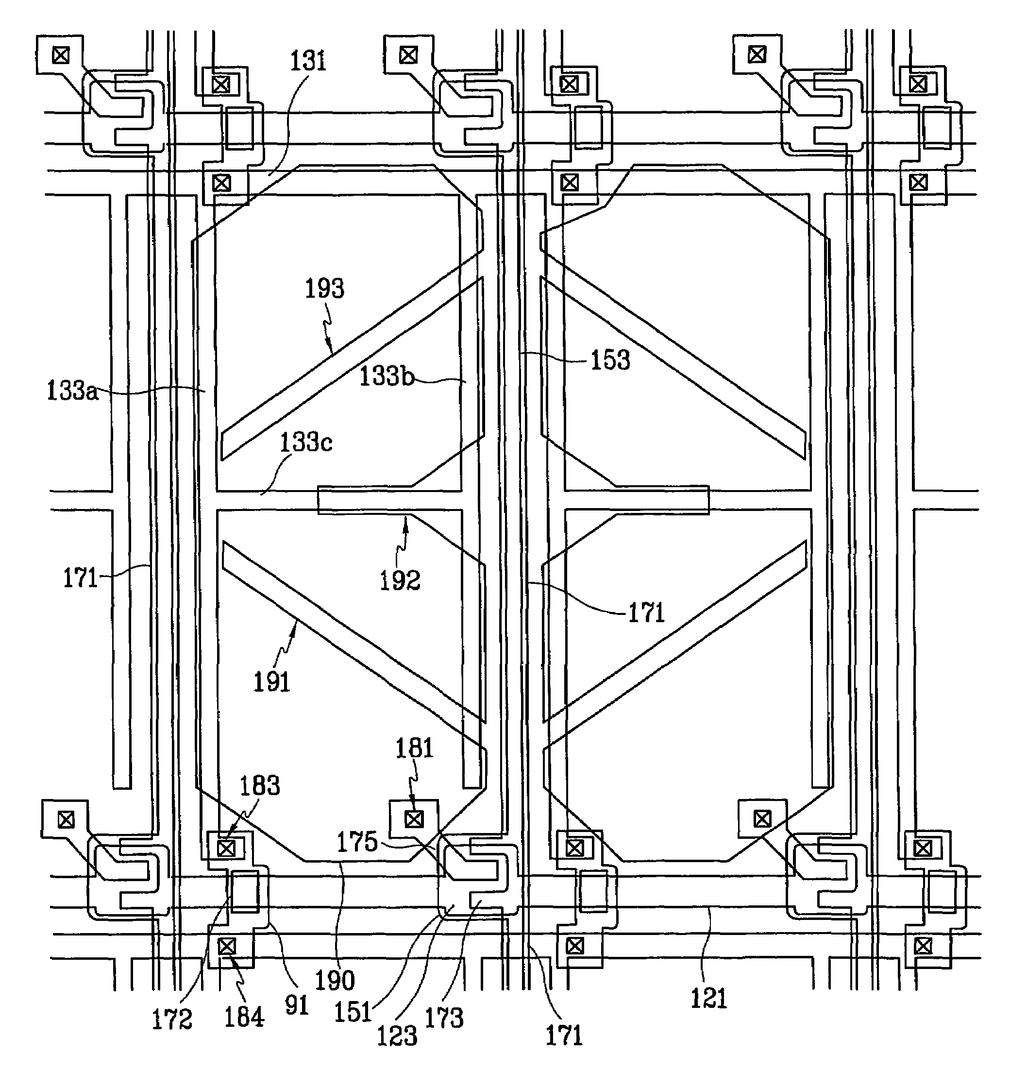
[0040]An LCD will be described more in detail.

[0041]A plurality of gate lines 121 extending substantially in a transverse direction are formed on a lower insulating substrate 110. A plurality of expansions of each gate line 121 form a plurality of gate electrodes 123. A plurality of storage electrode lines 131 extending substantially parallel to the gate lines 121 are also formed on the insulating substrate 110. A plurality of pairs of storage electrodes 133a and 133b extending in a longitudinal direction are branched from each storage electrode line 131 are connected to each other via a storage electrode 133c extending in the transverse direction. The number of the storage electrode lines 131 may be two or more. The gate lines 121, the gate electrodes 123, the storage electrode lines 131 and the storage electrodes 133 are preferably made of metal such as Al or Cr. They include either a single layer or double layers preferably including sequentially deposited Cr and Al layers. Alte...

second embodiment

[0056]FIG. 6 is a sectional view of an LCD according to the present invention.

[0057]An LCD according to the second embodiment is different from the LCD according to the first embodiment in that a plurality of protuberances 281 are provided as a domain partitioning means instead of the cutouts of a reference electrode. Alternatively, a plurality of protuberances 281 is provided on a plurality of pixel electrodes 190, or the cutouts 191, 192 and 193 the pixel electrodes 190 are substituted with a plurality of protuberances.

[0058]FIG. 7 is a layout view of a TFT array panel for an LCD according to a third embodiment of the present invention, and FIG. 8 is a layout view of a color filter panel according to the third embodiment of the present invention, and FIG. 9 is a layout view of an LCD according to the third embodiment of the present invention.

[0059]A TFT array panel of an LCD according to the third embodiment of the present invention has substantially the same structure as that acc...

third embodiment

[0060]The cutouts 191, 192 and 193 of each pixel electrode 190 of the TFT array panel for an LCD include a central cutout 192 extending substantially along a transverse center line of the pixel electrode 190 and then forking into upper and lower branches diverging obliquely and two oblique cutouts 191 and 193 extending in oblique directions and located respectively in a lower half and an upper half of the pixel electrode 190.

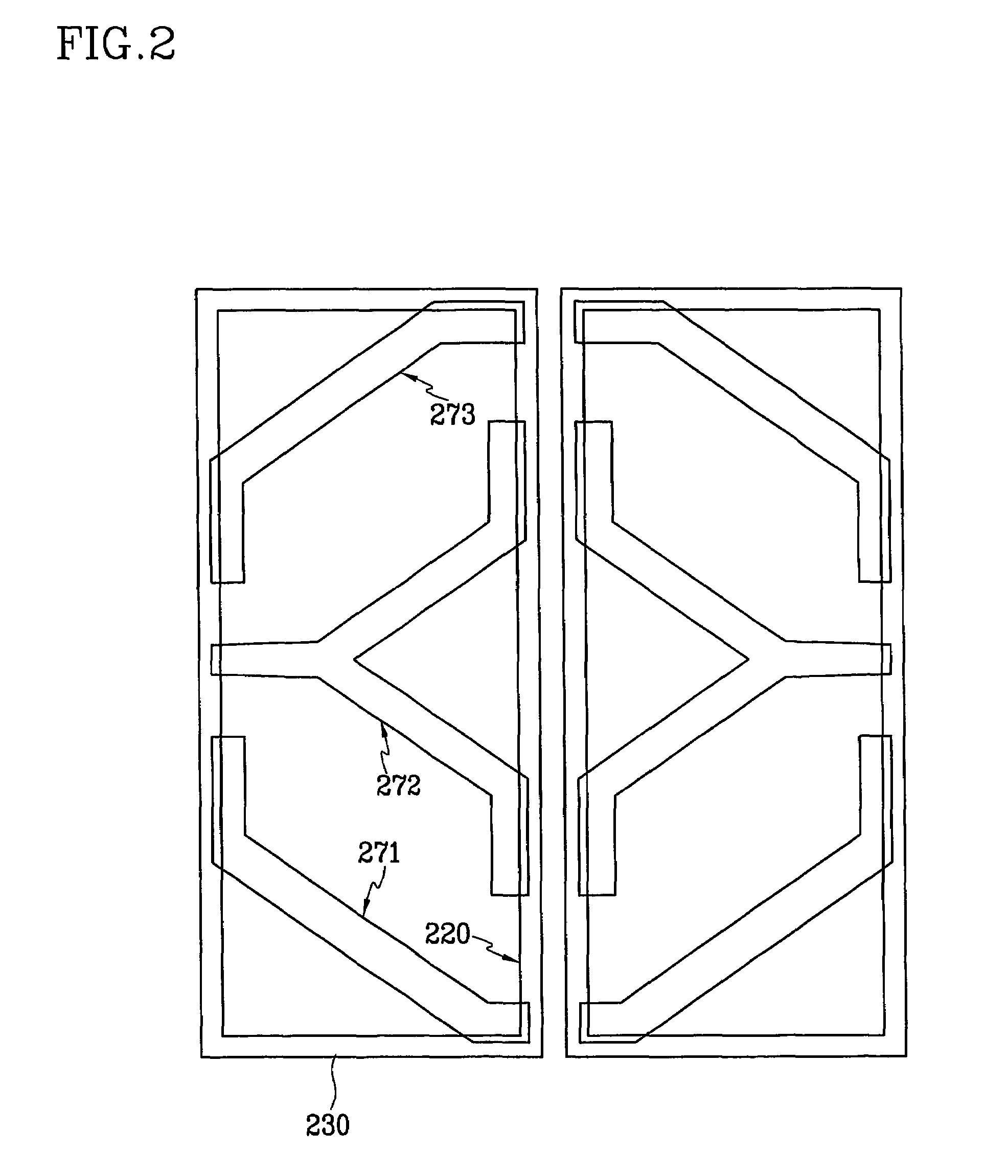
[0061]A color filter panel has a black matrix 220 and a plurality of color filters 230, which have substantially the same configurations as that according to the first embodiment. However, the color filter array panel has a reference electrode with a plurality of first to five cutouts 271-275 having the shapes different from those according to the first embodiment. Only the arrangement of the cutouts 271-275 will be described now.

[0062]Each first cutout 271 and each third cutout 273 traverse a pixel area in oblique directions and the cutouts 271 and 273 in two ...


PUM

PropertyMeasurementUnit
thicknessaaaaaaaaaa
temperatureaaaaaaaaaa
dielectricaaaaaaaaaa

Abstract

A plurality of gate lines and a plurality of data lines intersecting each other are formed on a first insulating substrate having a plurality of first cutouts are formed on the respective pixel areas defined by the data lines and the gate lines. A thin film transistor is connected to each pixel electrode. A reference electrode having a plurality of second cutouts is formed on a second substrate opposite the first substrate. The first cutouts and the second cutouts in the adjacent two pixel areas opposite each other with respect to one data line have an inversion symmetry with respect to the data line.

Description

BACKGROUND OF THE INVENTION[0001](a) Field of the Invention[0002]The present invention relates to a vertically aligned mode liquid crystal display, and, in particular, to a vertically aligned mode liquid crystal display including an electrode with cutouts for securing wide viewing angle.[0003](b) Description of Related Art[0004]A typical liquid crystal display (“LCD”) includes an upper panel with a reference electrode and color filters, a lower panel with thin film transistors (“TFTs”) and pixel electrodes and a liquid crystal layer with dielectric anisotropy interposed therebetween, and displays desired images by applying different voltages to the reference electrode and the pixel electrodes to generate electric field in the liquid crystal layer, which changes the orientations of liquid crystal molecules to control the light transmittance.[0005]Among these LCDs, a vertically aligned mode LCD (referred to as a “VALCD” hereinafter), which aligns the major axes of the liquid crystal m...

Claims


Application Information

Patent Timeline
Patent Type & Authority Patents(United States)
IPC IPC(8): G02F1/1343G02F1/1333G02F1/1337G02F1/1368G02F1/139H01L21/336H01L29/786
CPCG02F1/133707G02F1/1393G02F1/1343
Inventor JUN, SAHNG-IKPARK, WOON-YONG
Owner TCL CHINA STAR OPTOELECTRONICS TECH CO LTD
Why Eureka
Try Eureka