Integrated coherent optical detector

a coherent optical and detector technology, applied in the field of integrated devices, can solve the problem that the approach is not applicable to active integrated devices, and achieve the effect of maximizing the intensity of output signals

Inactive Publication Date: 2009-01-27
CELIGHT
View PDF2 Cites 38 Cited by
  • Summary
  • Abstract
  • Description
  • Claims
  • Application Information

AI Technical Summary

Benefits of technology

[0021]In another embodiment of the present invention, a method of the integrated device alignment uses the alignment system to precisely position the optical interface and the receiving unit. The method maximizes intensity of the output signal from the alignment waveguide by measuring current of the alignment photodiode.

Problems solved by technology

This approach is not applicable to active integrated devices.

Method used


Image

  • Integrated coherent optical detector
  • Integrated coherent optical detector
  • Integrated coherent optical detector

Examples


Embodiment Construction

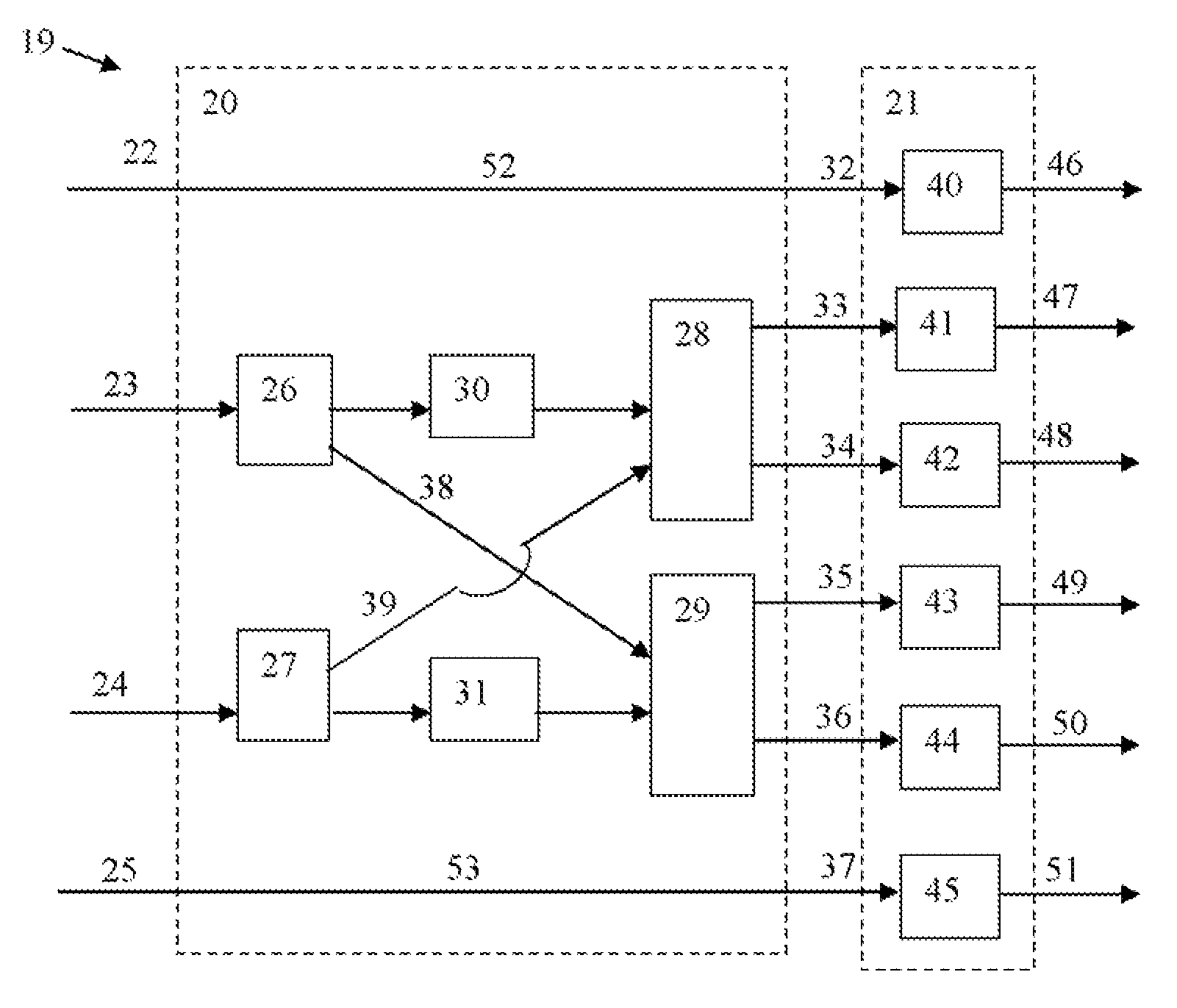
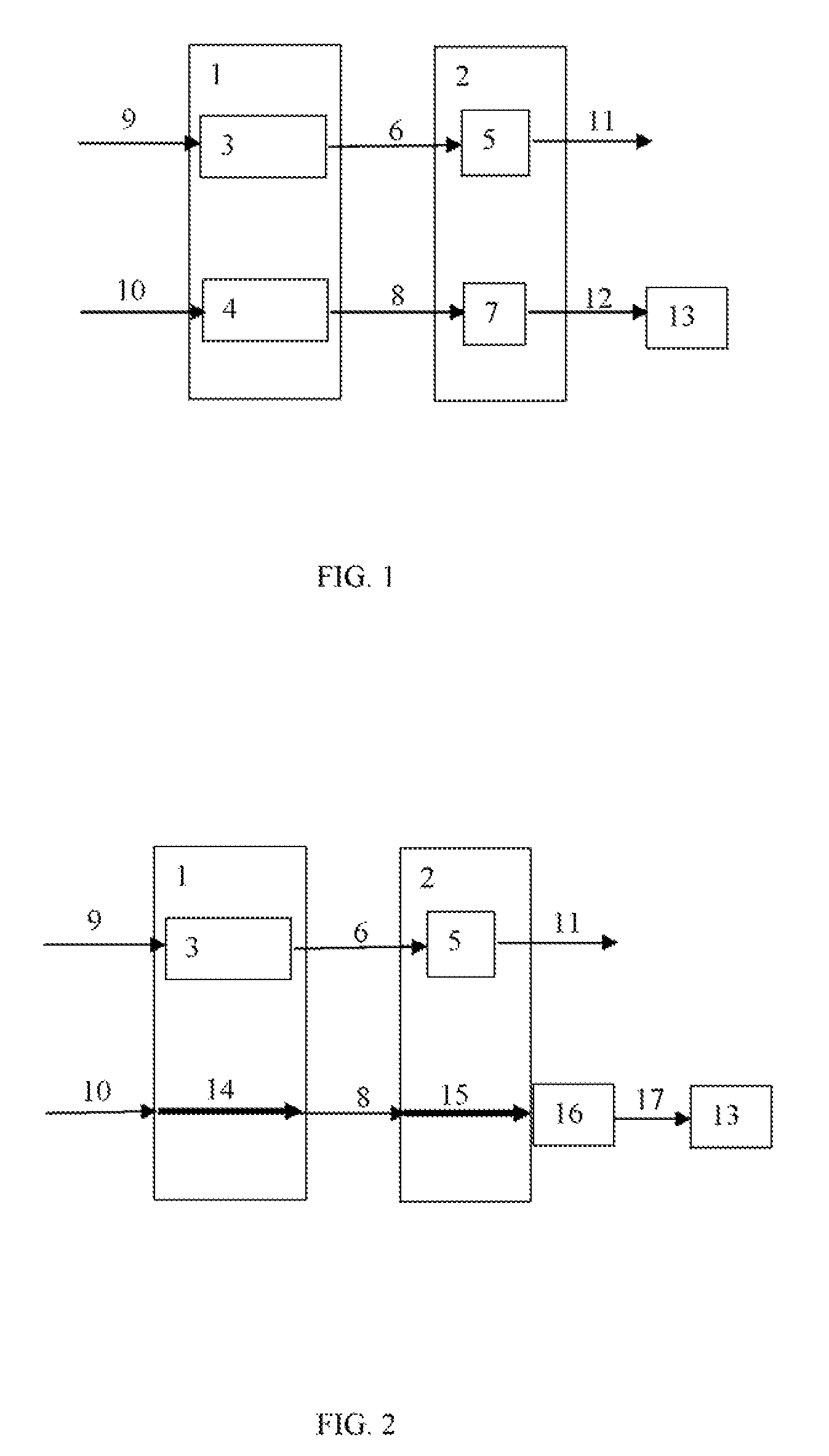
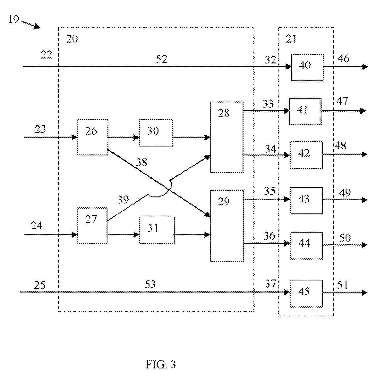
[0032]In one embodiment of the present invention, an optical device, such as optical device illustrated in FIG. 1, hereafter referred as Optical Device, is provided that includes an optical interface 1 and a receiving unit 2.

[0033]The interface 1 includes an interface circuit 3 and a first alignment system 4. The receiving unit 2 contains a receiving circuit 5 for receiving at least one output signal 6 from the interface circuit 3 and a second alignment system 7 for receiving at least one output signal 8 from the first alignment system 4.

[0034]In one embodiment the interface circuit is an electro-optical device. It is known that alignment of output waveguides from the electro-optical (EO) device with inputs of receiving circuit is a complicated task. The inputs have to be positioned and attached prior to the EO device activation.

[0035]In case when the receiving circuit 5 contains a set of photodiodes, the alignment is still very difficult. A simple procedure of directing light throu...


PUM


Abstract

The present invention provides an integrated device and a method of its fabrication and use. Two parts of the device each having an electronic circuit are aligned adjacent to each other with an accuracy of at least 1 micron. An alignment system includes two parts: a first part integrated with the first electronic circuit of the integrated device on the first substrate and a second part integrated with the second electronic circuit of the integrated device on the second substrate. The second part of alignment system includes at least one photodiode. The maximal value of the photodiode current indicates the best alignment of two parts of the integrated device. In one embodiment the integrated device is a coherent optical detector for high speed optical communications and chemical sensing. In another embodiment the integrated optical device is a coherent optical detector operating in two polarization states of light.

Description

CROSS-REFERENCE TO RELATED APPLICATIONS[0001]This application is a continuation-in-part of Ser. No. 10 / 669,130 filed Sep. 22, 2003 now U.S. Pat. No. 7,327,913. This application is also a continuation-in-part of Ser. No. 11 / 610,964, filed Dec. 14, 2006 now U.S. Pat. No. 7,397,979 and Ser. No. 10 / 613,772, filed Jul. 2, 2003 now U.S. Pat. No. 7,272,271, all of which applications are fully incorporated herein by reference.FIELD OF THE INVENTION[0002]This invention relates generally to integrated devices and their fabrication and use, and more particularly to electro-optical receiving devices being used for coherent detection of optical signals in optical communications and remote sensing.BACKGROUND OF THE INVENTION[0003]Lasers are widely used today in fiber and free space segments for high data rate communication links, remote sensing applications (LIDAR) and more. In these applications the modulated light signal is modulated using electro-optical modulators and demodulated using, usual...

Claims


Application Information

Patent Timeline
Patent Type & Authority Patents(United States)
IPC IPC(8): G02B6/12
CPCG02B6/4225
Inventor ACHIAM, YAAKOVSHPANTZER, ISAACGREENBLATT, ARTHURHARSTON, GEOFFREYKAPLAN, ARKADYCHO, PAK SHING
Owner CELIGHT
Why Eureka
Try Eureka