Method of aligning an optical fiber, method of manufacturing a semiconductor laser module, and semiconductor laser module

a technology of laser module and optical fiber, which is applied in the direction of semiconductor lasers, instruments, record information storage, etc., can solve the problems of large size of semiconductor laser modules, long manufacturing time, complicated manufacturing process, etc., and achieve the effect of easy alignmen

Inactive Publication Date: 2005-06-16
FURUKAWA ELECTRIC CO LTD
View PDF3 Cites 5 Cited by
  • Summary
  • Abstract
  • Description
  • Claims
  • Application Information

AI Technical Summary

Benefits of technology

[0035] a first step of moving and positioning said optical fiber such that an intensity of said combined laser beams optically coupled to said optical fiber is maximized; and
[0037] Since the optical length of the optical path between the first and second lenses differs between two laser beams passing through the polarization-combiner, the two laser beams form beam waists at different positions in the axial direction of the optical fiber optically downstream of the second lens. If the optical fiber is moved between these positions, the efficiency at which the laser beams are coupled to the optical fiber is changed, a point is found at which the laser beams coupled to the optical fiber have an equal intensity, and thereby a degree of polarization of the combined beam can be low.
[0039] Since the beam waists are formed between the first lens and the second lens, the beam diameter can be smaller between the first lens and the second lens, and since the propagation length reduces necessary to reach a given divergent width between the two laser beams, the distance to the optical fiber can be shortened. In addition, optical parts used between the first lens and the second lens can be reduced in size.
[0058] Forming the beam waists between the first lens and the second lens makes the beam diameter smaller between the first lens and the second lens, and reduces the propagation length necessary to reach a predetermined divergent width between the two laser beams. Therefore, the length of the laser module can be shortened. The use of small-sized optical parts reduces the laser module in size.
[0060] Since the two laser beams that have exited the first lens propagate while being separated from each other symmetrically with respect to the central axis of the first lens and then the prism collimates the optical axes of the two laser beams, the polarization-combiner can be designed and processed with ease, and the lens, the prism and the polarization-combiner can easily be positioned with respect to the laser device. Furthermore, fixing the polarization-combiner and the prism to the same single holder facilitates alignment of the prism and the polarization-combiner greatly.
[0070] Since the polarization synthesis means and the reflector are fixed by the same single holder, the polarization synthesis means and the reflector can be aligned very easily.

Problems solved by technology

However, in the prior art 1, the lenses have to be aligned with respect to the respective laser beams emitted from the two semiconductor laser devices, which makes the manufacturing process complicated and requires a long time to manufacture.
It is difficult in practical point of view, however, to dispose the polarization rotator and the polarization element between the semiconductor laser device and the lens.
Adopting a larger lens would create a larger space, but this approach will have a problem that a package needs to be larger in size than currently used, resulting in the semiconductor laser module being larger in size.
The configuration has a problem that it is unsuitable for mass production since semiconductor laser devices are large in size and not obtained in large quantity from a single wafer.
Narrowing a spacing between the stripes of the semiconductor laser device in order to obviate the above problem would need to accompany downsizing of the lenses, making it difficult to separate the laser beams emitted from the stripes and polarization-combining or optical combining of the beams that follows.
Further, the method of manufacturing the semiconductor laser module according to the Prior Art cannot always prevent the degree of polarization from exceeding an acceptable level due to a difference in characteristics (laser emission angle (FFP: Far Field Pattern) from an emission end face), optical output, and wavelength, as well as temperature dependency of these characteristics) between two semiconductor laser devices, a difference in placement of optical parts, a warped package, and the like.

Method used


Image

  • Method of aligning an optical fiber, method of manufacturing a semiconductor laser module, and semiconductor laser module
  • Method of aligning an optical fiber, method of manufacturing a semiconductor laser module, and semiconductor laser module
  • Method of aligning an optical fiber, method of manufacturing a semiconductor laser module, and semiconductor laser module

Examples


first embodiment

[0137] (First Embodiment)

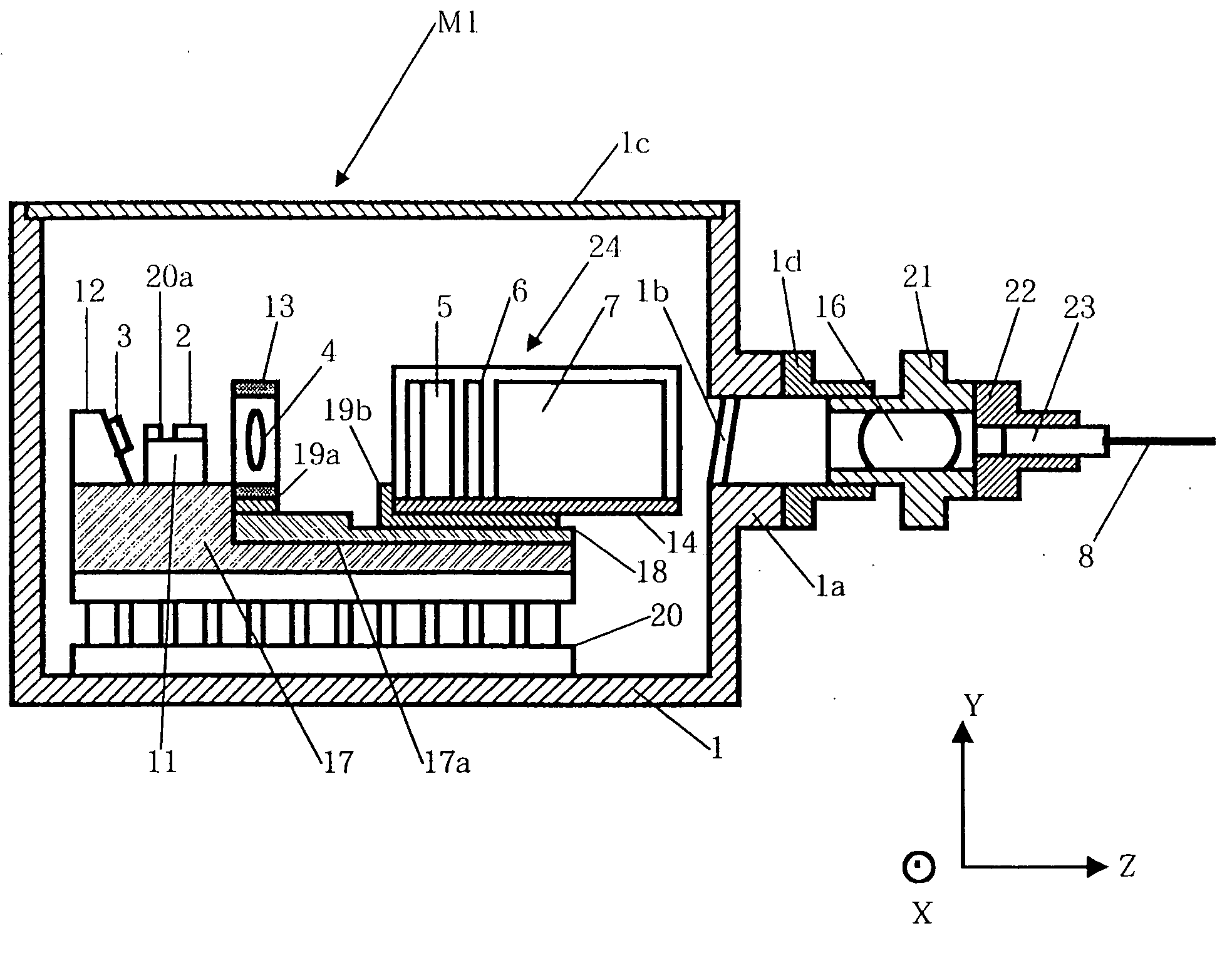
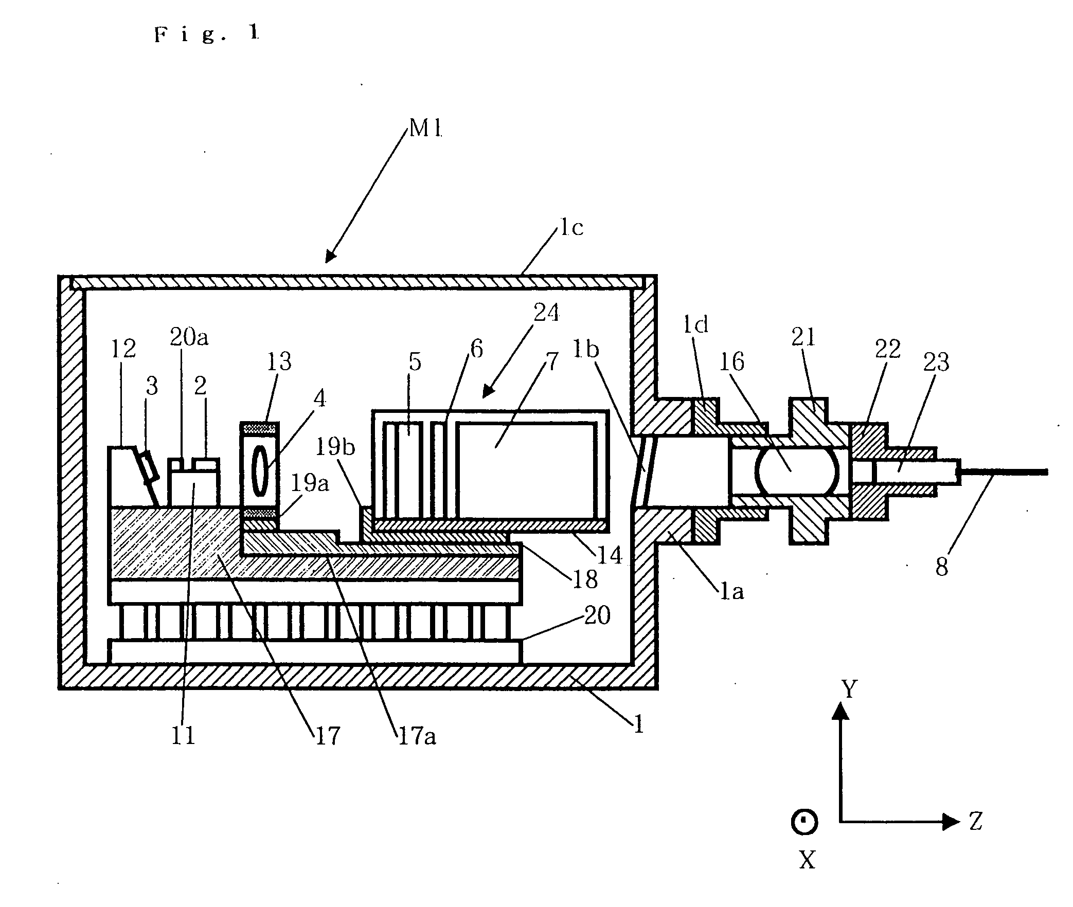
[0138]FIG. 1 is a side sectional view showing a configuration of a semiconductor laser module manufactured by a method in accordance with a first embodiment of the present invention.

[0139] As shown in FIG. 1, a semiconductor laser module M1 manufactured by the method in accordance with the first embodiment of the present invention includes a package 1 whose interior is hermetically sealed, a semiconductor laser device 2 encased in the package 1 for emitting laser beam, a photodiode (light receiving element) 3, a first lens 4, a prism 5, a half-wave plate (a polarization rotating element) 6, a PBC 7 as a polarization synthesis elemenet, and an optical fiber 8.

[0140] The semiconductor laser device 2 includes, as shown in FIG. 5, a first stripe 9 and a second stripe 10 disposed at a distance on the same plane and extending in parallel in the longitudinal direction. The semiconductor laser device 2 emits a first laser beam K1 and a second laser beam K2 respect...

second embodiment

[0179] (Second Embodiment)

[0180]FIG. 9 is a plan view showing a semiconductor laser module M6 according to a second embodiment of the present invention. As shown in FIG. 9, the semiconductor laser module M2 according to the second embodiment of the present invention includes: a first semiconductor laser device 38 for emitting a first laser beam K1; a second semiconductor laser device 39 for emitting a second laser beam K2; two first lenses 40 and 41 on which the two laser beams K1 and K2 emitted from the two semiconductor laser devices 38 and 39 are incident, respectively; a cube beam splitter 42 as a polarization synthesis elemenet; and a mirror 43 as a reflector that reflects the laser beam K2 toward the cube beam splitter 42. The other structure is the same as that of the first embodiment.

[0181] In the second embodiment of the present invention, the second laser beam K2 enters the cube beam splitter 42 through the mirror 43. Therefore, a light path of the first laser beam K1 and...

third embodiment

[0191] (Third Embodiment)

[0192]FIG. 10 is a plan view showing a semiconductor laser module according to a third embodiment of the present invention.

[0193] A semiconductor laser module M3 according to the third embodiment includes: a semiconductor laser device 46 which is an array laser equipped with a first stripe 44 and a second stripe 45 that are parallel to each other across a gap of about 500 μm; a first lens 47 for receiving the first laser beam K1 that is emitted from the first stripe 44; and a first lens 48 for receiving the second laser beam K2 that is emitted from the second stripe 45. The other structure is the same as that of the first embodiment.

[0194] The third embodiment uses the PBC 7 as in the first embodiment. Therefore, a light path of the first laser beam K1 differs from a light path of the second laser beam K2 in optical length, and the distance α1 between the first stripe 44 and the first lens 47 differs from the distance α2 between the second stripe 45 and th...


PUM

PropertyMeasurementUnit
refractive index n2aaaaaaaaaa
length L2aaaaaaaaaa

Abstract

A method of aligning an optical fiber according to the present invention has a first step of aligning an optical fiber by moving the optical fiber and finding a position that maximizes the power of beam outputted from the optical fiber with the use of a power meter, and a second step of moving and aligning the optical fiber in the optical axis direction (direction Z) from the position in which the optical fiber has been as a result of the alignment in the first step in a manner that makes the degree of polarization of two laser beams K1 and K2 equal to or lower than a given level with the use of a polarimeter.

Description

[0001] This application is a continuation of international application serial No. PCT / JP02 / 09539 filed on Sep. 17, 2002, the entire content of which is incorporated herein by reference.TECHNICAL FIELD [0002] The present invention relates to a method of aligning an optical fiber, a method of manufacturing a semiconductor laser module, and a semiconductor laser module. More specifically, the invention relates to a method of aligning an optical fiber, a method of manufacturing a semiconductor laser module, and a semiconductor laser module in which two laser beams are polarization-combined before received by an optical fiber. BACKGROUND ART [0003] With progress in the optical communications based on a dense wavelength division multiplexing transmission system over the recent years, a higher output is increasingly demanded to a pumping light source used for the optical amplifier. [0004] Further, a greater expectation is recently given to a Raman amplifier as an amplifier for amplifying t...

Claims


Application Information

Patent Timeline
Patent Type & Authority Applications(United States)
IPC IPC(8): G02B6/34G02B6/42G11B7/00H01S5/00H01S5/02H01S5/022H01S5/024H01S5/0683H01S5/40
CPCG02B6/2713G02B6/2766G02B6/4204G02B6/4214G02B6/4225H01S5/005H01S5/4031H01S5/02284H01S5/02415H01S5/02438H01S5/0683H01S5/4012H01S5/02248H01S5/02325H01S5/02251
Inventor NAKAE, MASASHIKIMURA, TOSHIO
Owner FURUKAWA ELECTRIC CO LTD
Why Eureka
Try Eureka