Optical reflectance proximity sensor

a technology of optical reflectance and proximity sensor, which is applied in the field of optical reflectance proximity sensor and improved reflectance sensor, can solve the problems of high power consumption, large volume, and large active reflectance sensor, and achieve the effect of improving the accuracy of optical reflectance sensor

Active Publication Date: 2009-02-03
SILICON LAB INC
View PDF33 Cites 214 Cited by
  • Summary
  • Abstract
  • Description
  • Claims
  • Application Information

AI Technical Summary

Benefits of technology

[0033]In another aspect of the method, there are more than one transmitting diode and in step (c), each of the transmitting diodes is caused to transmit separately from the other diodes. In one aspect of the method, in step (

Problems solved by technology

Although these classic echo-based sensors provide relatively accurate distance and speed information, they can, depending on the application, be expensive, bulky, may consume high power, and/or may require very high frequency technologies to be successful.
Even these types of active reflectance sensors, although fairly small and robust, have been too expensive for consumer applications and consequently have found applications mostly in the industrial and commercial markets.
However, they are too large for many consumer products because they require a collecting lens and a photodiode of several centimeters in diameter to gather a sufficient signal to sense changes in the ambient background visible to the sensor.
Moreover, a major handicap of such sensors is a la

Method used


Image

  • Optical reflectance proximity sensor
  • Optical reflectance proximity sensor
  • Optical reflectance proximity sensor

Examples


Embodiment Construction

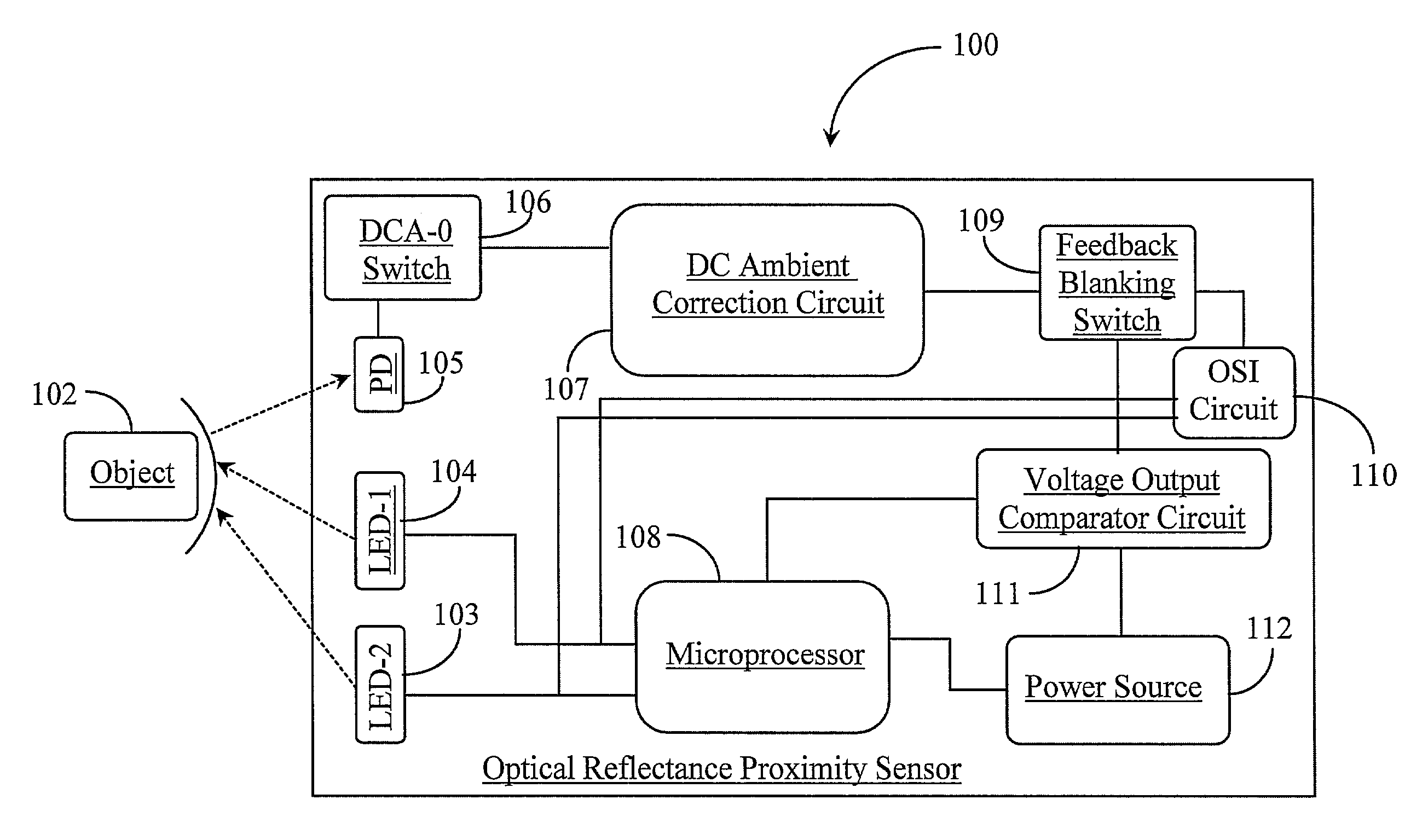
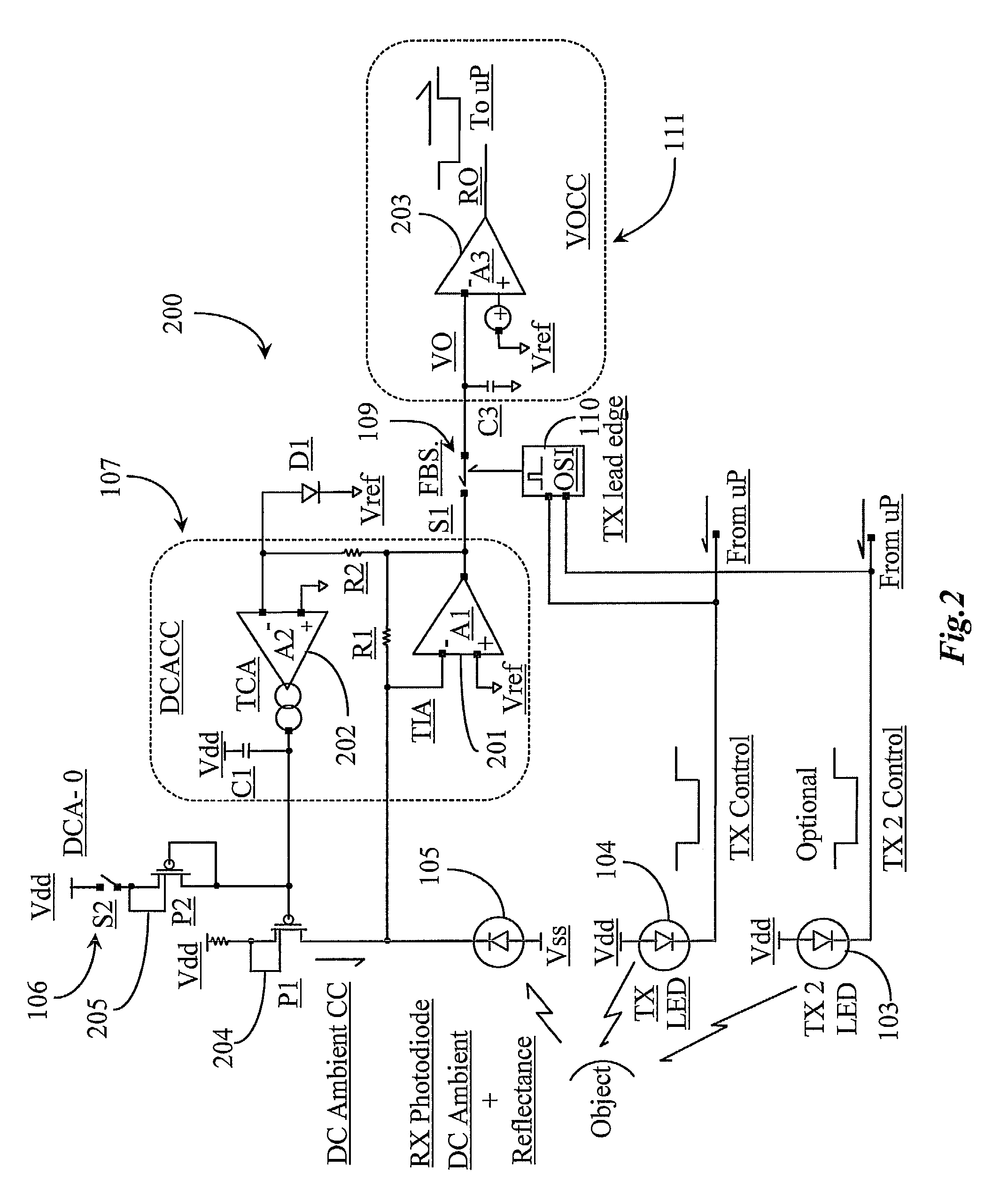
[0057]The inventors provide an improved active optical reflectance proximity sensor architecture that may include a first-order, wide-loop DC ambient correction circuit that along with an optional feedback-immunity circuit among other added functions to achieve very high reflectance sensitivity in the presence of large DC and other ambient noises. The sensor is enabled using an economically viable architecture allowing for sensor implementation in the form of very low power on-off proximity sensors and more sophisticated analog-output proximity sensors that can be easily interfaced to microprocessors, or may stand alone, in some applications, to facilitate a wide range of proximity applications. The invention is described in detail in the various embodiments presented herein.

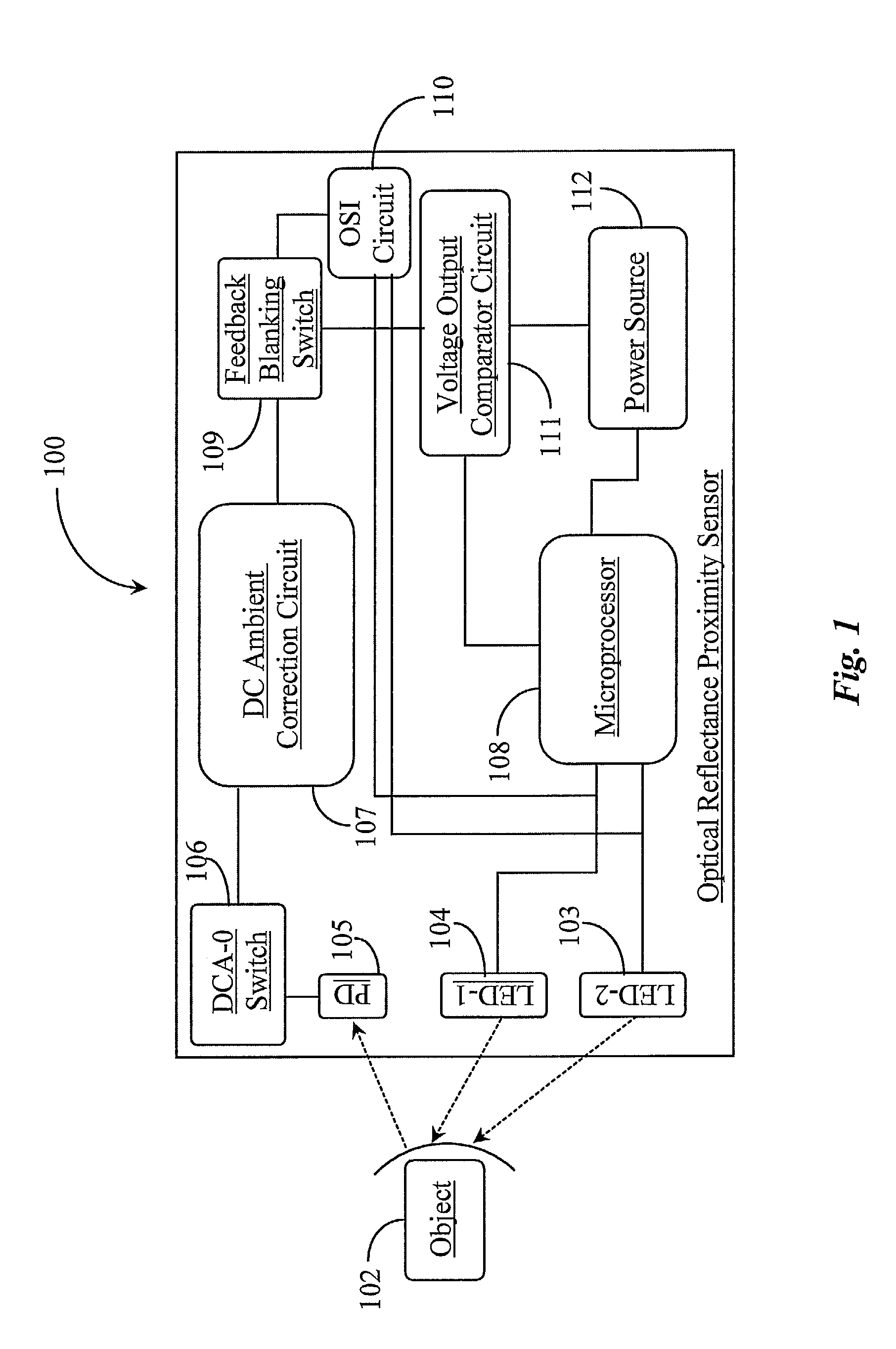
[0058]FIG. 1 is a block diagram of an optical reflectance proximity sensor 100 according to an embodiment of the present invention. Proximity sensor 100 is configured as an “active” optical reflectance proximity...


PUM


Abstract

A method for calibrating an optical reflectance proximity sensor and then measuring proximity in a repeating cycle or on demand, the sensor including one or more wavelength transmitting diodes, one or more wavelength receiving diodes, an ambient correction circuit, and a comparator circuit, and further teaching steps for powering on the sensor, canceling the ambient signal during a calibration period, transmitting wavelengths to and receiving reflectance from an object in the path of the transmitted wavelengths, and measuring a reflectance pulse width and comparing the value to a preset value to determine proximity.

Description

CROSS-REFERENCE TO RELATED APPLICATIONS[0001]The present invention is related in part to a U.S. Pat. No. 5,864,591 entitled “Apparatus and Method for Suppression of Feedback in a Communications Receiver” issued on Jan. 26, 1999 to Wayne T. Holcombe, and in part to a U.S. Pat. No. 6,240,283 entitled “Apparatus and Method for Suppression of Feedback in a Communications Receiver”, issued on May 29, 2001; both disclosures included herein at least by reference.BACKGROUND OF THE INVENTION[0002]1. Field of the Invention[0003]The present invention is in the field of electronic sensors and pertains particularly to an improved reflectance sensor usable in various commercial and consumer applications.[0004]2. Discussion of the State of the Art[0005]In the field of sensory devices, more particularly electronic sensors, proximity sensing and motion detection are regimens that provide contact-less control and object detection useful in a large variety of consumer, industrial, and security applica...

Claims


Application Information

Patent Timeline
IPC IPC(8): G01C3/08
CPCG01C3/08G01S7/497G01S17/026H03K17/941G01S7/4815H03K2217/94026G01S17/04
Inventor HOLCOMBE, WAYNE THOMASSVAJDA, MIROSLAV
Owner SILICON LAB INC
Why Eureka
Try Eureka