Method for manufacturing thin film transistor in display device

a technology of thin film transistor and display device, which is applied in the direction of transistors, semiconductor devices, electrical equipment, etc., can solve the problems of inability to contribute to a drastic reduction in the number of steps, inability to manufacture thin film transistors, and theoretical difficulties, so as to achieve high-reliability display, reduce material loss and cost, and good adhesion

Inactive Publication Date: 2009-02-17
SEMICON ENERGY LAB CO LTD
View PDF16 Cites 24 Cited by
  • Summary
  • Abstract
  • Description
  • Claims
  • Application Information

AI Technical Summary

Benefits of technology

[0008]It is an object of the present invention to reduce the number of photolithography steps in the manufacturing process of a TFT, an electronic circuit using the TFT, and a display device formed using the TFT, and to simplify the manufacturing process. It is a further object of the present invention to provide a technique by the TFT, the electronic circuit, and the display device can be manufactured even over a large substrate with a side of more than one meter with higher yield at lower cost.
[0009]It is another object of the present invention to provide a technique by which wiring patterns and the like constituting a part of a display device can be formed with good adhesion to manufacture a highly reliable display device.
[0010]In the invention, an object on which a component is formed refers to as a formation subject. The component constituting a part of a thin film transistor, a display device or the like is formed by adding (mixing) a material which is the same as at least one of substances forming the surface of the formation subject, which has good adhesion to the formation subject in the component to improve adhesion between the component and the formation subject. Further, insulating layer formed over the component is formed with a laminate of a first insulating layer containing an organic material and a second insulating layer containing an inorganic material; thus, the insulating layer sufficiently covers irregularities on the surface of the component, and is also dense enough so as to be reliable as an insulating layer.
[0033]According to the present invention, a thin film transistor or a component forming a display device can be formed with a desired pattern and good adhesion. Further, the material loss and costs can be reduced. Hence, a high-performance and highly reliable display device can be manufactured with high yield.

Problems solved by technology

Therefore, as the number of the photolithography steps is increased, the manufacturing cost is inevitably increased.
However, in the technique disclosed in Reference 1, only some of the plural photolithography steps in a TFT manufacturing process are replaced by printing method, and no contribution is made to a drastic reduction in the number of steps.
It is theoretically difficult, from a technical standpoint, to expose a large substrate which is more than one meter on a side to light all at once using the light exposure apparatus.

Method used


Image

  • Method for manufacturing thin film transistor in display device
  • Method for manufacturing thin film transistor in display device
  • Method for manufacturing thin film transistor in display device

Examples


embodiment mode 3

[0161]An embodiment mode of the present invention will be described with reference to FIGS. 10A to 10D and FIGS. 11A and 11B. In this embodiment mode, a display device is manufactured using a top gate type (a staggered type) thin film transistor. An example of a liquid crystal display device using a liquid crystal material as a display element is shown. Accordingly, the same part or a part having similar function will not be repeatedly explained. FIGS. 10A to 10D and FIGS. 11A and 11B show cross-sectional views of the display device.

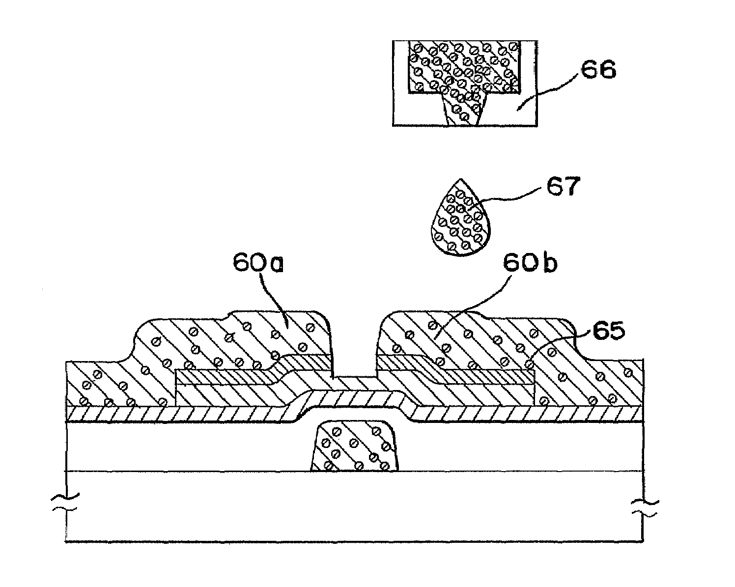
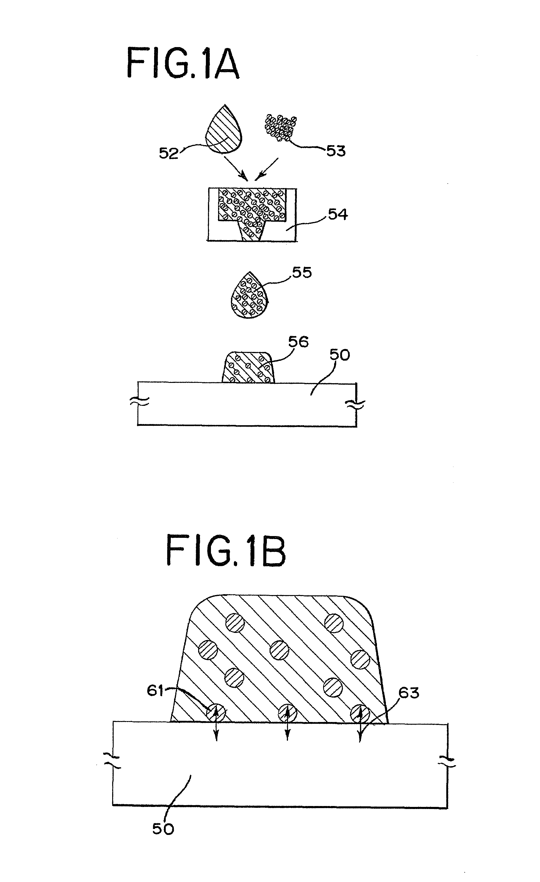
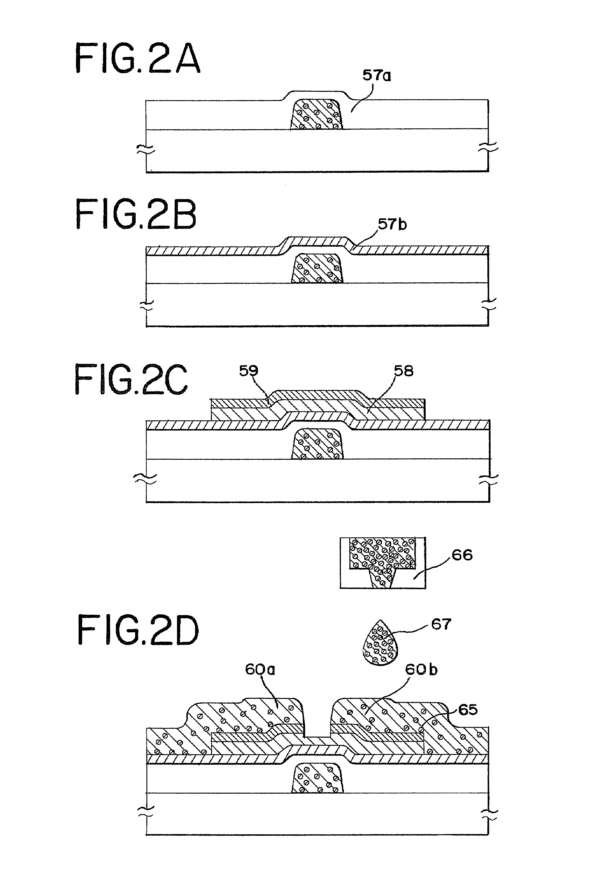
[0162]In this embodiment mode, a particle shape matter containing a material which is the same as at least one of the substances forming the formation subject surface is added (mixed) into a composition containing a conductive material to form a conductive layer. The matter containing a material which is the same as at least one of the substances forming the surface of the formation subject has a particle shape and may have a diameter of 100 nm or less, ...

embodiment mode 4

[0178]A thin film transistor can be formed by applying the present invention, and a display device can be formed with the use of the thin film transistor. In addition, when a light emitting element is used and an n-channel transistor is used as a transistor which drives the light emitting element, light emitted from the light emitting element performs any one of bottom emission, top emission, and dual emission. Here, a layered structure of a light emitting element corresponding to each emission will be described with reference to FIGS. 12A to 12C.

[0179]Further, in this embodiment mode, channel protective thin film transistors 461, 471, and 481 according to the present invention are used. The thin film transistor 481 is provided over a substrate 480 and includes a gate electrode layer 493, a first insulating layer 497a, a second insulating layer 497b, a semiconductor layer 494, an n-type semiconductor layer 495, a source / drain electrode layer 482, and a channel protective layer 496. ...

embodiment mode 5

[0210]In a display panel manufactured according to Embodiment Modes 2 to 4, as shown in FIG. 14B, a scan line driver circuit can be formed over a substrate 3700 by forming a semiconductor layer with a SAS.

[0211]FIG. 25 shows a block diagram of the scan line driver circuit including n-channel TFTs using a SAS in which electric field effect mobility of from 1 cm2 / V·sec to 15 cm2 / V·sec is obtained.

[0212]In FIG. 25, a block 500 corresponds to a pulse output circuit outputting a sampling pulse for one stage and a shift register includes n pulse outputting circuits. Reference numeral 901 denotes a buffer circuit and connected to a pixel 902.

[0213]FIG. 26 shows a specific structure of the block 500 which is a pulse output circuit, and the pulse output circuit includes n-channel TFTs 601 to 613. The size of the TFTs may be decided in consideration of the operation characteristics of the n-channel TFTs using a SAS. For example, when a channel length shall be 8 μm, the channel width can be se...


PUM


Abstract

The present invention provides a technique by which a component forming a display device, such as a wiring can be formed with good adhesion.In the invention, a component forming a thin film transistor, a display device, or the like is formed with a material which is the same as at least one of the substances forming the formation subject surface added (mixed); thus, adhesion between the component and the formation subject is improved. An insulating layer formed over the component is formed with a laminate of a first insulating layer containing an organic material and a second insulating layer containing an inorganic material; thus, the insulating layer sufficiently covers irregularities on the surface of the component, and is also dense enough so as to be reliable as an insulating layer.

Description

BACKGROUND OF THE INVENTION[0001]1. Field of the Invention[0002]The invention relates to a thin film transistor and a method for manufacturing the same, a display device and a method for manufacturing the same, and a television device using the above.[0003]2. Description of the Related Art[0004]A thin film transistor (hereinafter, referred to as a “TFT”) and an electronic circuit using the thin film transistor are manufactured by stacking various types of thin films of such as a semiconductor, an insulator, a conductor over a substrate and then, appropriately forming a predetermined pattern by photolithography. The photolithography is a technique of transferring a pattern of a circuit or the like formed with a material which does not transmit light over a transparent flat surface, referred to as a photomask, onto an objective substrate by utilizing light. The technique has been widely used in the manufacturing processes of a semiconductor integrated circuit and the like.[0005]In the...

Claims


Application Information

Patent Timeline
Patent Type & Authority Patents(United States)
IPC IPC(8): H01L21/00H01L21/44H01L21/84H01L21/77
CPCH01L27/1214H01L27/1292
Inventor MAEKAWA, SHINJI
Owner SEMICON ENERGY LAB CO LTD
Why Eureka
Try Eureka