Charge pump circuit and semiconductor device having the same

a technology of a pump circuit and a semiconductor device, applied in the direction of dc-dc conversion, power conversion systems, instruments, etc., can solve the problems of increasing the circuit area, reducing the yield, and dropping the output voltage, so as to improve the output current and output potential, reduce the circuit area, and reduce the power consumption

Inactive Publication Date: 2009-02-24
SEMICON ENERGY LAB CO LTD
View PDF10 Cites 57 Cited by
  • Summary
  • Abstract
  • Description
  • Claims
  • Application Information

AI Technical Summary

Benefits of technology

[0025]The present invention can provide a semiconductor device including a step-up or step-down circuit having a novel structure. Accordingly, a reduction in power consumption, an improvement in output current and output potential, and a reduction in circuit area due to a reduction in circuit scale can be realized.
[0026]In addition, since the charge pump circuit of the present invention can be formed using a thin film transistor, frequencies of clock signals of a liquid crystal display device, a display device including a light emitting element (hereinafter also referred to as a light emitting device), or another display device can be selected in accordance with display mode, and the power consumption of the display device can be reduced.
[0027]Moreover, an external circuit can be simplified by forming the charge pump circuit and a circuit which is needed for a semiconductor device over the same substrate. Therefore, the number of circuit parts can be reduced, and cost reduction can be realized.

Problems solved by technology

A conventional charge pump has a structure in which two diodes are connected in series and has a problem of a drop in output voltage by the same amount as a threshold voltage of the diode.
Accordingly, a circuit scale is increased, which leads to an increase in circuit area, a decrease in yield, and an increase in power consumption.
In addition, a conventional charge pump switching element as described above has the following problem when incorporated in a display device.
Therefore, the conventional charge pump switching element has a problem of loss of power source stability when a current load is heavy and an output current is increased.

Method used


Image

  • Charge pump circuit and semiconductor device having the same
  • Charge pump circuit and semiconductor device having the same
  • Charge pump circuit and semiconductor device having the same

Examples


embodiment mode 1

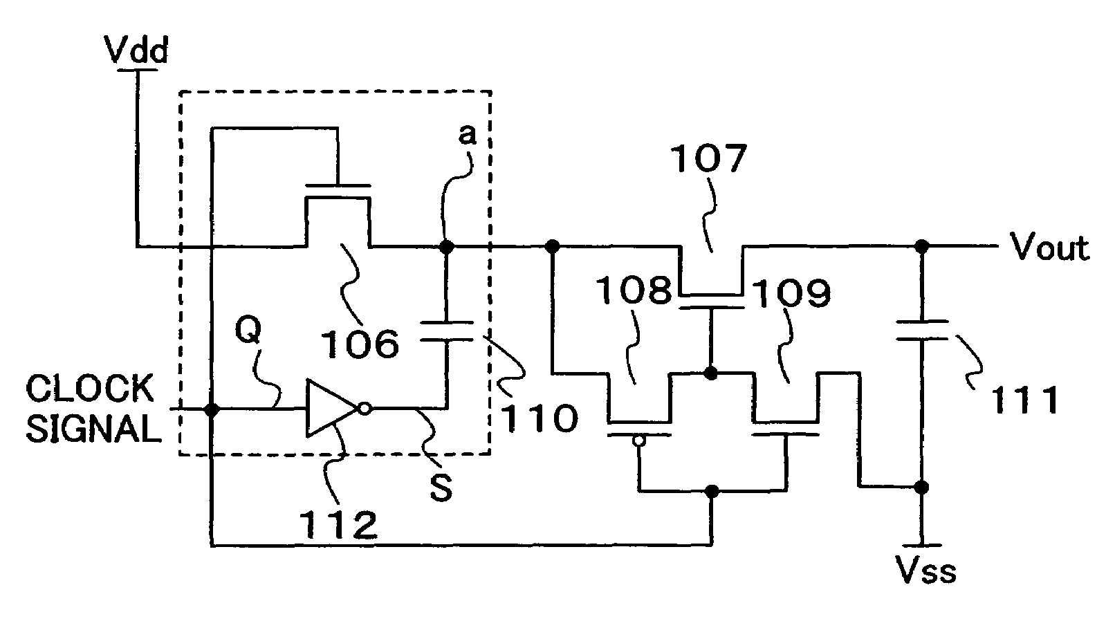
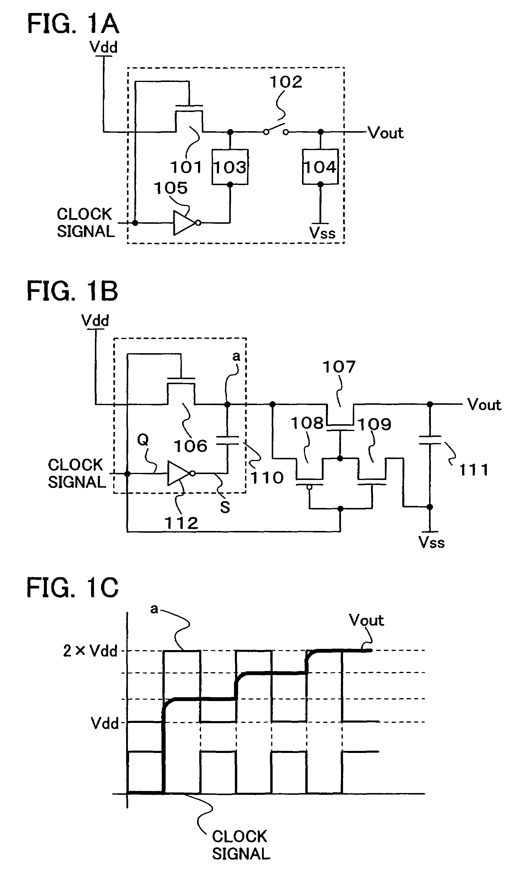
[0045]FIG. 1B shows the structure of a charge pump circuit of this embodiment mode of the present invention. The charge pump circuit of this embodiment mode of the present invention includes elements such as a first transistor 106, a second transistor 107, a third transistor 108, a fourth transistor 109, a first capacitor 110, a second capacitor 111, and an inverter 112. In this embodiment mode, the conductivity of the first transistor 106, the second transistor 107, and the fourth transistor 109 is set to an n-channel type. In addition, that of the third transistor 108 is set to a p-channel type. Further, one feature of the first transistor 106 and the second transistor 107 is to be normally on.

[0046]Next, the connection relation of each element is explained.

[0047]A first electrode of the first transistor 106 is connected to Vdd at a high-level potential. An output side (point S) of the inverter 112 is connected through the first capacitor 110 to a second electrode of the first tra...

embodiment mode 2

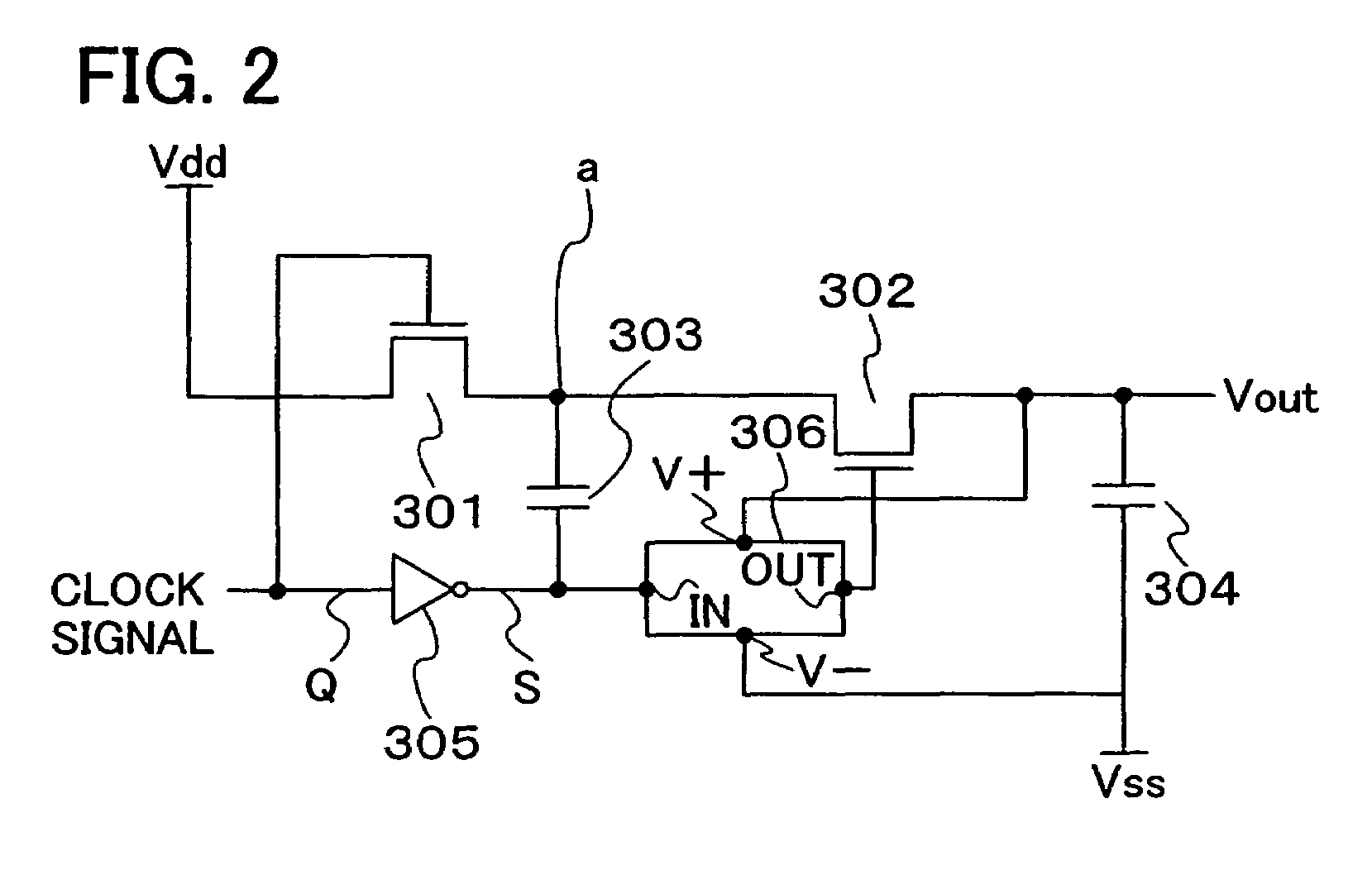
[0058]FIG. 2 shows an example of a structure of another charge pump circuit. The charge pump circuit includes a first transistor 301, a second transistor 302, a first capacitor 303, a second capacitor 304, and an inverter 305, and further includes a step-up circuit 306, which is different from FIG. 1B. The first transistor 301 and the second transistor 302 are set to have n-channel type conductivity. Further, a feature is that the first transistor 301 and the second transistor 302 are set to be normally on.

[0059]Next, the connection relation of each element is explained. A first electrode of the first transistor 301 is connected to Vdd at a high-level potential. An output side (point S) of the inverter 305 is connected through the first capacitor 303 to a second electrode of the first transistor 301 and a first electrode of the second transistor 302. The connection point is indicated by “a” in FIG. 2 and is hereinafter referred to as a “node a”. In addition, the output side (point S...

embodiment mode 3

[0070]This embodiment mode explains the structure and operation of a charge pump, which are different from those in the above embodiment modes.

[0071]FIG. 3A shows the structure of a charge pump circuit of this embodiment mode of the present invention.

[0072]The charge pump shown in FIG. 3A includes a first transistor 201, a second transistor 202, a third transistor 203, a first capacitor 204, a second capacitor 205, a third capacitor 206, a first inverter 207, a second inverter 208, a third inverter 209, and a fourth inverter 230, and the first transistor 201 and the third transistor 203 are set to have n-channel type conductivity and the second transistor 202 is set to have p-channel type conductivity. Further, a feature is that the first transistor 201 and the third transistor 203 are normally on.

[0073]Next, the connection relation of each element is explained.

[0074]First electrodes of the first transistor 201 and the third transistor 203 are connected to Vdd at a high-level potent...


PUM


Abstract

A conventional charge pump circuit requires a step-up circuit or the like for turning on or off a transistor. Therefore, it has a problem of an increase in circuit scale, which leads to increases in circuit area and power consumption. One feature is to provide a charge pump circuit including a first transistor, a switch, a first capacitor, a second capacitor, and an inverter, in which one electrode of the first transistor is connected to a first potential, an output side of the inverter is connected to the other electrode of the first transistor and one side of the switch through the first capacitor, the other side of the switch is connected to a second potential through the second capacitor.

Description

BACKGROUND OF THE INVENTION[0001]1. Field of the Invention[0002]The present invention relates to a charge pump circuit having a novel structure, more specifically, a semiconductor device using a charge pump circuit as a step-up circuit or a step-down circuit.[0003]2. Description of the Related Art[0004]A step-up circuit includes that using a coil and that using a capacitor. The one using a capacitor is generally called a charge pump. A conventional charge pump has a structure in which two diodes are connected in series and has a problem of a drop in output voltage by the same amount as a threshold voltage of the diode. In order to solve this problem, another structure using a switch instead of a diode has been proposed (see References 1: Japanese Published Patent Application No. 2001-136733, Reference 2: Japanese Published Patent Application No. H07-327357, and Reference 3: Japanese Published Patent Application No. H07-099772).[0005]In order to realize the circuit disclosed in Refer...

Claims


Application Information

Patent Timeline
Patent Type & Authority Patents(United States)
IPC IPC(8): G05F1/10
CPCH02M3/07G11C5/14
Inventor IWABUCHI, TOMOYUKIUENO, TATSURO
Owner SEMICON ENERGY LAB CO LTD
Why Eureka
Try Eureka