Decoupling capacitor control circuit and method for enhanced ESD performance

a control circuit and capacitor technology, applied in the direction of circuit arrangements, electrical equipment, circuit arrangements responsive to excess voltage, etc., can solve the problems of introduction of unwanted inductance, and improper operation of electronic circuits

Active Publication Date: 2009-02-24
BAE SYST INFORMATION & ELECTRONICS SYST INTEGRATION INC
View PDF6 Cites 21 Cited by
  • Summary
  • Abstract
  • Description
  • Claims
  • Application Information

AI Technical Summary

Problems solved by technology

Transients or other types of noise on the supply voltage can result in improper operation of the electronic circuitry.
Regardless of the source of the noise, the noise can introduce transients on the supply voltage of the electronic circuitry that causes improper operation of the electronic circuitry.
These external decoupling capacitors occupied valuable space on the printed circuit board, introduced unwanted inductance in the path of the supply voltage, and required additional manufacturing operations to position and connect the capacitors to the printer circuit board.
As a result, as with all components being formed on a semiconductor die, there is a probability that some of these internal decoupling capacitors will be defective.
If a decoupling capacitor is formed utilizing the oxide of such a thin region, the capacitor may be defective since the undesirably thin oxide may result in a short circuit between the conductive plates of the capacitor.
Such a defective capacitor results in an undesirable consumption of power since the defective capacitor presents a short circuit between the supply voltage and ground for the corresponding chip.
If the defective capacitors were to remain connected to the power supply, then the corresponding chip may consume an undesirably high amount of power.
This could result in the failure or turning off of a power supply providing power to the chip due to excessive current draw from the power supply.
Even where the excess current does not result in the power supply failing or turning off, it could result in an undesirable reduction in the supply voltage that could cause chips on the printed circuit board to operate improperly.
Either situation is obviously undesirable, with the turning off or shutting down of the power supply rendering electronic circuitry including the chip unusable and a lower power supply voltage similarly being undesirable since such a lower voltage could compromise the proper operation of the chip, as will be appreciated by those skilled in the art.
More specifically, ESD events may result in transients on the supply voltage such that the reduced overall decoupling capacitance due to defective capacitors 102 may result in inadequate suppression of such transients and thereby result in damage to the associated chip due to the transients.
This reduced overall decoupling capacitance means the magnitude of an ESD transient voltage on the supply voltage plane will have a larger value than if all good decoupling capacitors 302 were properly connected, which could damage circuitry in the chip.
In practice, however, even though a transient from an ESD event will be transmitted to the gate of the transistor 304A via the resistor 308A this transient may not be sufficient to turn ON the transistor.

Method used


Image

  • Decoupling capacitor control circuit and method for enhanced ESD performance
  • Decoupling capacitor control circuit and method for enhanced ESD performance
  • Decoupling capacitor control circuit and method for enhanced ESD performance

Examples


Embodiment Construction

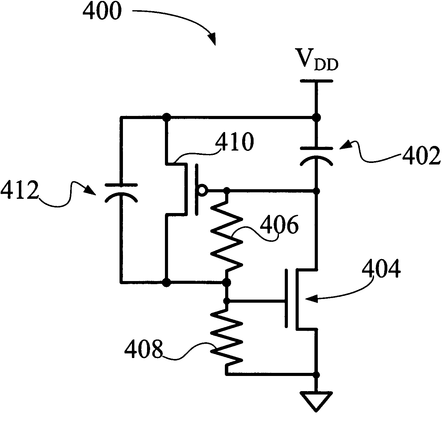
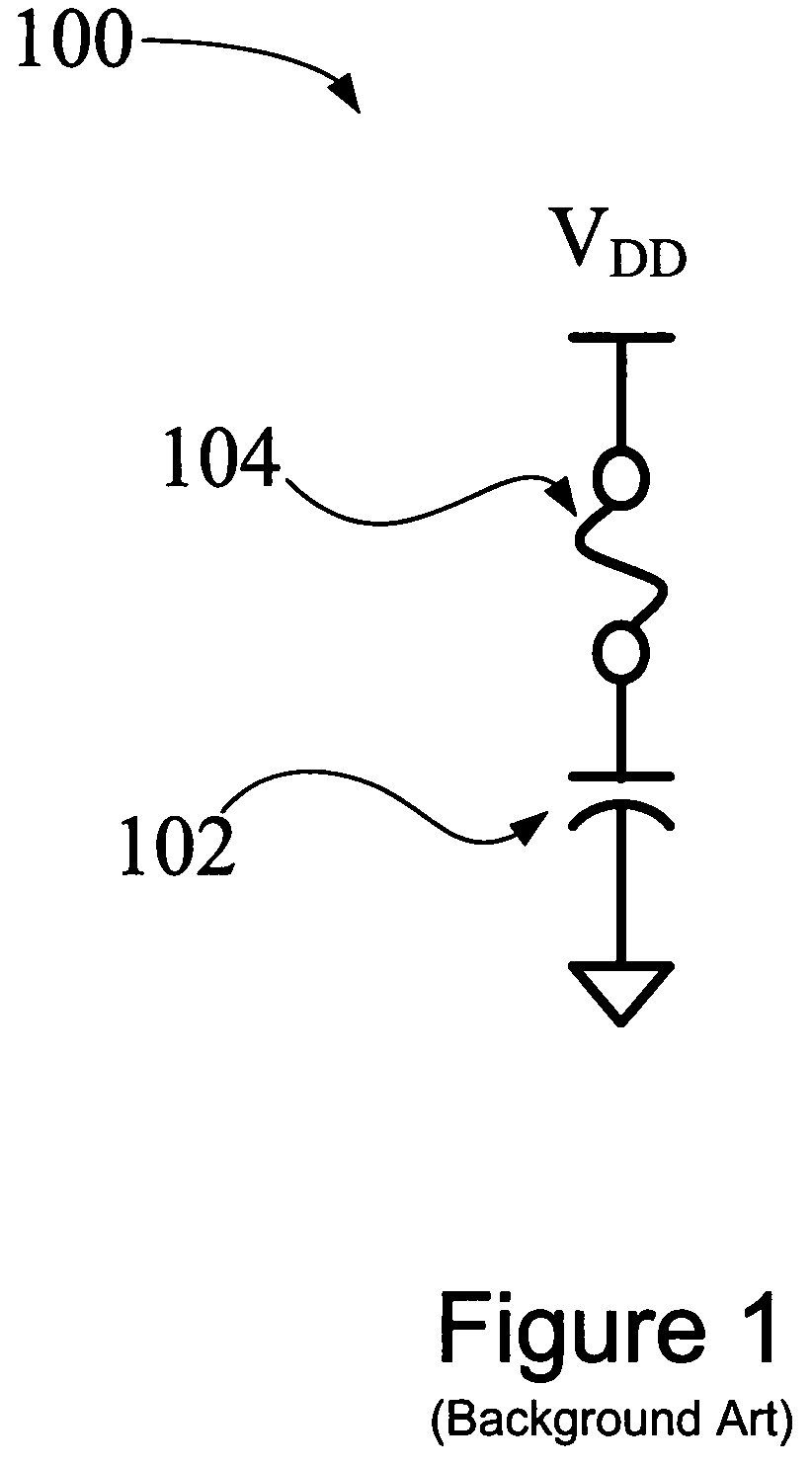
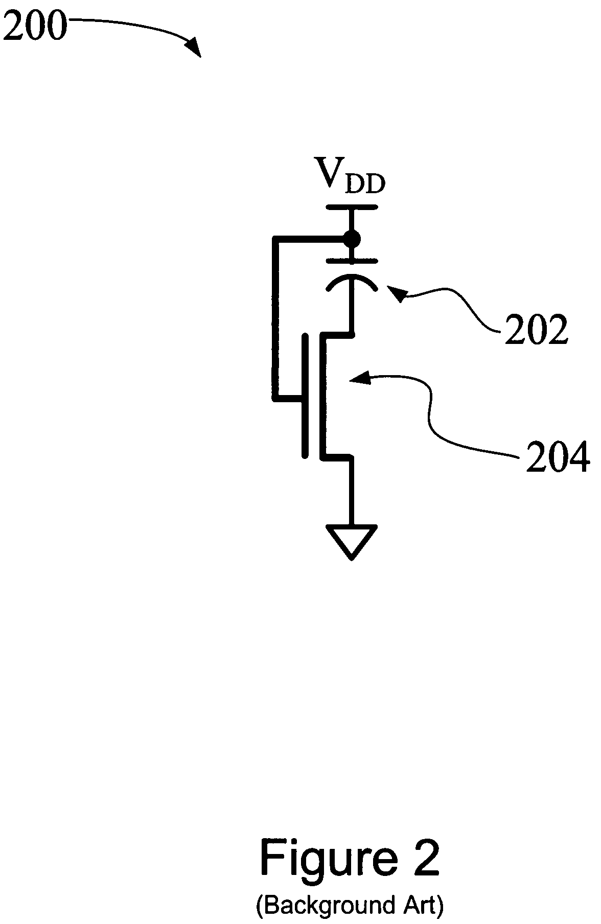
[0026]In the following description, certain details are set forth in conjunction with the described embodiments of the present invention to provide a sufficient understanding of the invention. One skilled in the art will appreciate, however, that the invention may be practiced without these particular details. Furthermore, one skilled in the art will appreciate that the example embodiments described below do not limit the scope of the present invention, and will also understand that various modifications, equivalents, and combinations of the disclosed embodiments and components of such embodiments are within the scope of the present invention. Embodiments including fewer than all the components of any of the respective described embodiments may also be within the scope of the present invention although not expressly described in detail below. Finally, the operation of well known components and / or processes has not been shown or described in detail below to avoid unnecessarily obscur...


PUM


Abstract

A decoupling capacitor control circuit is configured to be coupled between supply voltage and reference voltage planes. The control circuit includes a decoupling capacitor having a first node configured to be coupled to the supply voltage plane and having a second node. A first switching element has a first signal node coupled to the second node of the decoupling capacitor and has a second signal node and a control node. A second switching element has a first signal node coupled to the first node of the decoupling capacitor and has a second signal node coupled to the control node of the first switching element, and has a control node. A biasing circuit is coupled to the control nodes of the first and second switching elements. The biasing circuit activates both switching elements when the decoupling capacitor is not defective and deactivates both switching elements when the decoupling capacitor is defective.

Description

TECHNICAL FIELD[0001]The present invention relates generally to integrated circuits, and more specifically to electrostatic discharge (ESD) protection for integrated circuits.BACKGROUND OF THE INVENTION[0002]In electronic devices a supply voltage must be provided to supply power for the associated electronic circuitry to operate. Transients or other types of noise on the supply voltage can result in improper operation of the electronic circuitry. Noise can result from a variety of different sources, such as adjacent electronic circuitry, high power electronic devices where relatively high currents are being switched, or electrostatic discharge (“ESD”) events. Regardless of the source of the noise, the noise can introduce transients on the supply voltage of the electronic circuitry that causes improper operation of the electronic circuitry. To prevent such transients from adversely affecting the operation of the electronic circuitry, decoupling capacitors are connected between ground...

Claims


Application Information

Patent Timeline
Patent Type & Authority Patents(United States)
IPC IPC(8): H02H3/22
CPCH01L27/0266
Inventor TODD, RONALD C.
Owner BAE SYST INFORMATION & ELECTRONICS SYST INTEGRATION INC
Why Eureka
Try Eureka