Low power zones for programmable logic devices

a programmable logic and low power zone technology, applied in the field of integrated circuit (ic) device power supply distribution, can solve the problems of unused resources consuming static power, fpga devices typically exhibit greater static power consumption than dedicated logic devices,

Active Publication Date: 2009-03-03
XILINX INC
View PDF58 Cites 20 Cited by
  • Summary
  • Abstract
  • Description
  • Claims
  • Application Information

AI Technical Summary

Benefits of technology

[0007]A method and apparatus are disclosed that may significantly reduce static power consumption in an integrated circuit (IC) device such as a PLD by disabling unused or inactive resources without adversely affecting operation of the enabled resources. In accordance with the present invention, unused and / or inactive resources of the device may be disabled to reduce power consumption and then isolated from enabled (e.g., active) resources of the device to prevent invalid data signals from propagating from the disabled resources to the enabled resources.
[0008]For some embodiments, the device's resources are divided into a plurality of logic blocks that may be selectively disabled and isolated from each other. For one embodiment, each logic block is selectively coupled to a voltage supply by a corresponding switch element, and is selectively coupled to one or more other logic blocks by one or more corresponding signal isolation circuits. The switch elements and the signal isolation circuits may be controlled using corresponding power control and signal isolation control signals provided by an isolation control circuit. For one embodiment, asserting a power control signal turns on a switch element to enable the corresponding logic block, de-asserting the power control signal turns off the switch element to disable the logic block, asserting a signal isolation control signal turns on a signal isolation circuit to facilitate the exchange of data signals between the logic block and other device resources, and de-asserting the signal isolation control signal turns off the signal isolation circuit to prevent the exchange of data signals between the logic block and other device resources. In this manner, the signal isolation circuits may isolate disabled logic blocks from enabled logic blocks to prevent the transmission of invalid data signals from disabled logic blocks to enabled logic blocks.
[0011]For other embodiments, the device may include a non-volatile memory to store configuration data for the logic blocks, and also include a configuration control circuit that provides configuration data to one or more logic blocks that have been disabled and subsequently re-enabled. In this manner, the re-enabled logic blocks may be re-configured using configuration data stored within the device when they are re-enabled for operation, thereby eliminating the need to re-configure the device from an external source.

Problems solved by technology

PLDs such as FPGA devices typically exhibit greater static power consumption than dedicated logic devices such as standard-cell application specific integrated circuits (ASICs).
One reason for the PLD's high power consumption is because while the PLD utilizes only a subset of its available resources for any given design, the unused resources nevertheless consume static power.
However, if the inactive resources are de-coupled from the voltage supply during PLD operation, resulting leakage currents in the disabled resources may cause internal logic nodes therein to discharge toward ground potential, which in turn may cause data signals at one or more outputs of the disabled resources to have indeterminate or invalid logic states.
If provided to the enabled (e.g., active) resources of the PLD, these invalid data signals may drive logic elements in the enabled resources to invalid states, and thereby cause the enabled resources to function improperly.

Method used


Image

  • Low power zones for programmable logic devices
  • Low power zones for programmable logic devices
  • Low power zones for programmable logic devices

Examples


Embodiment Construction

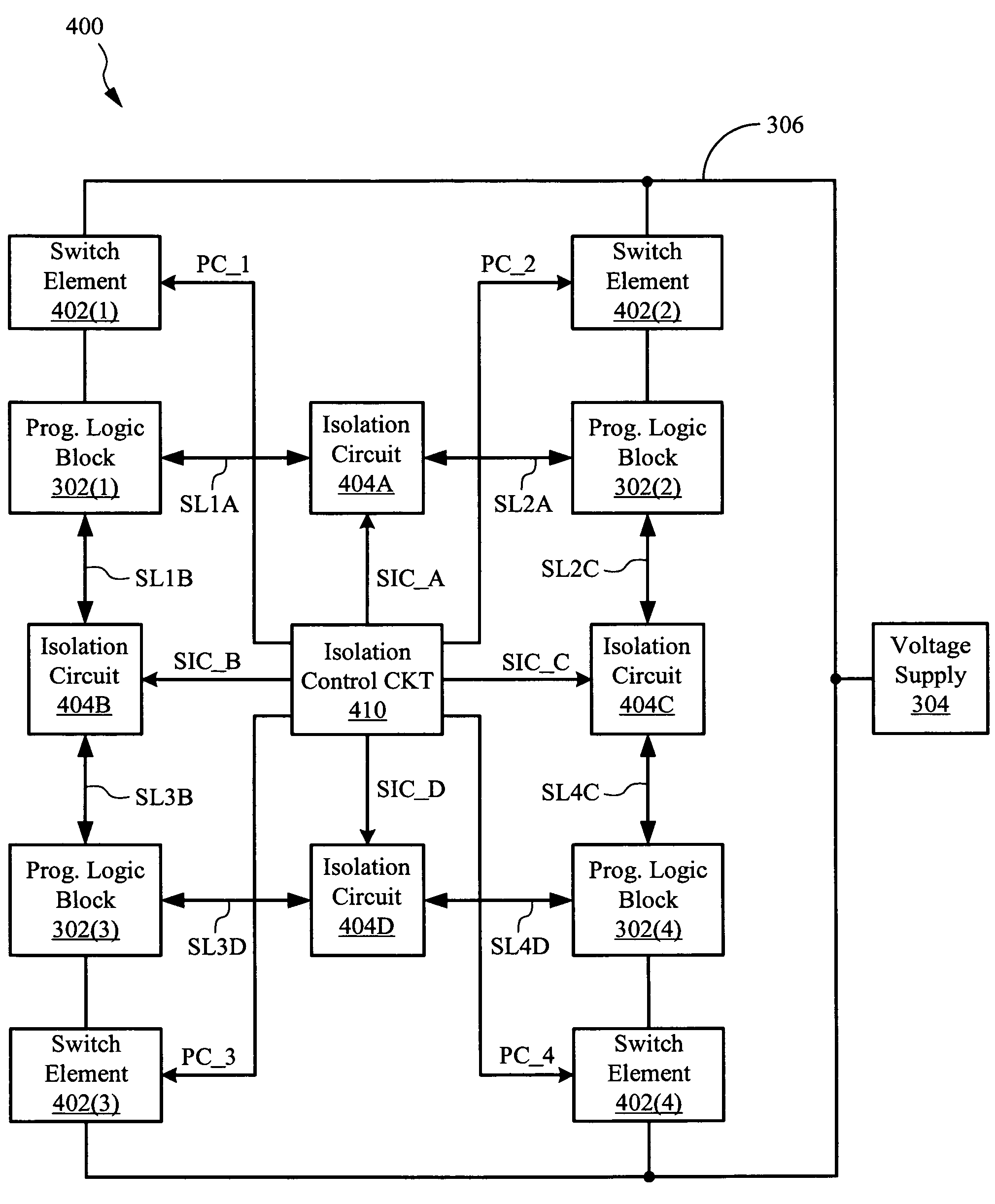
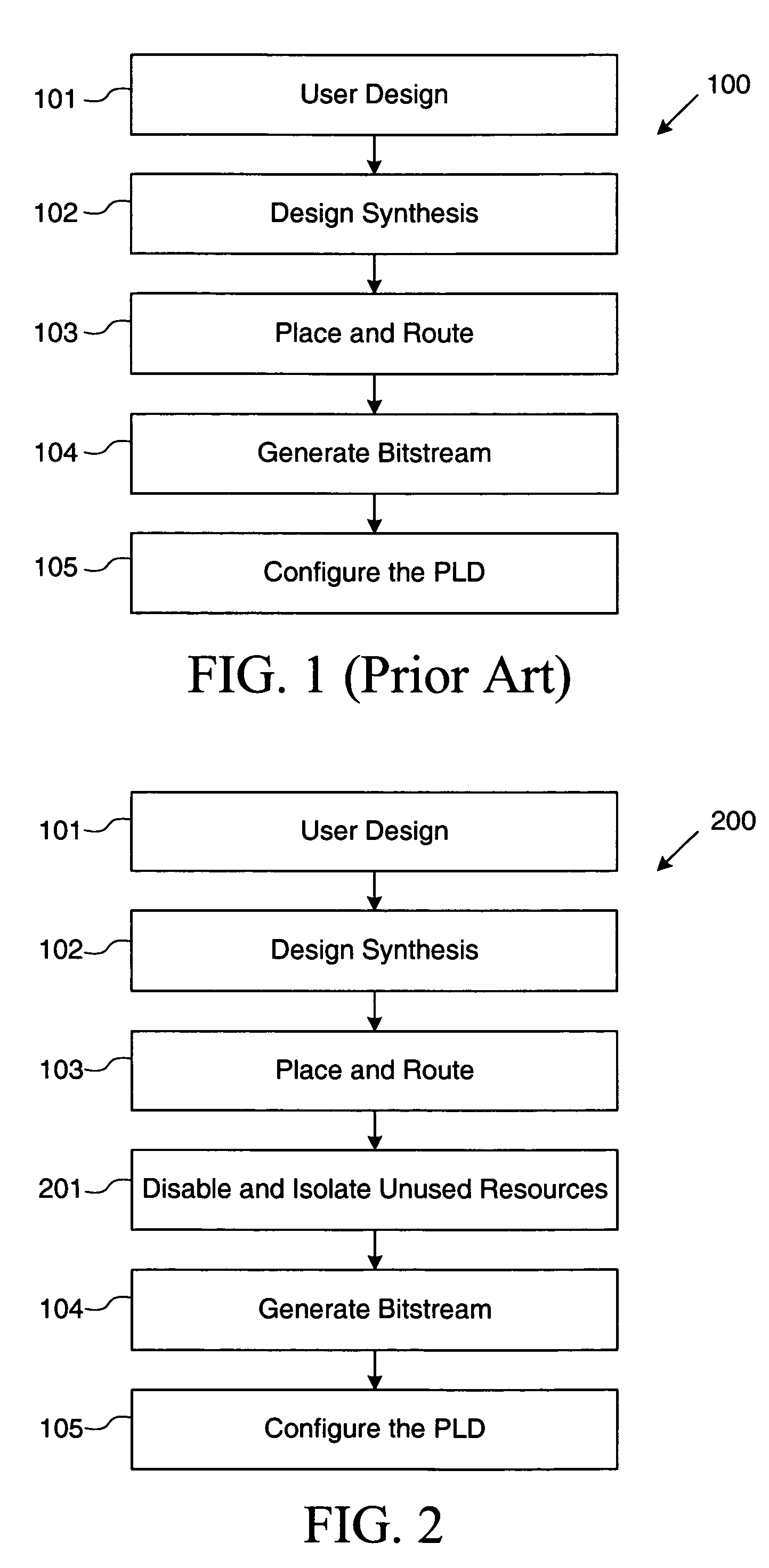
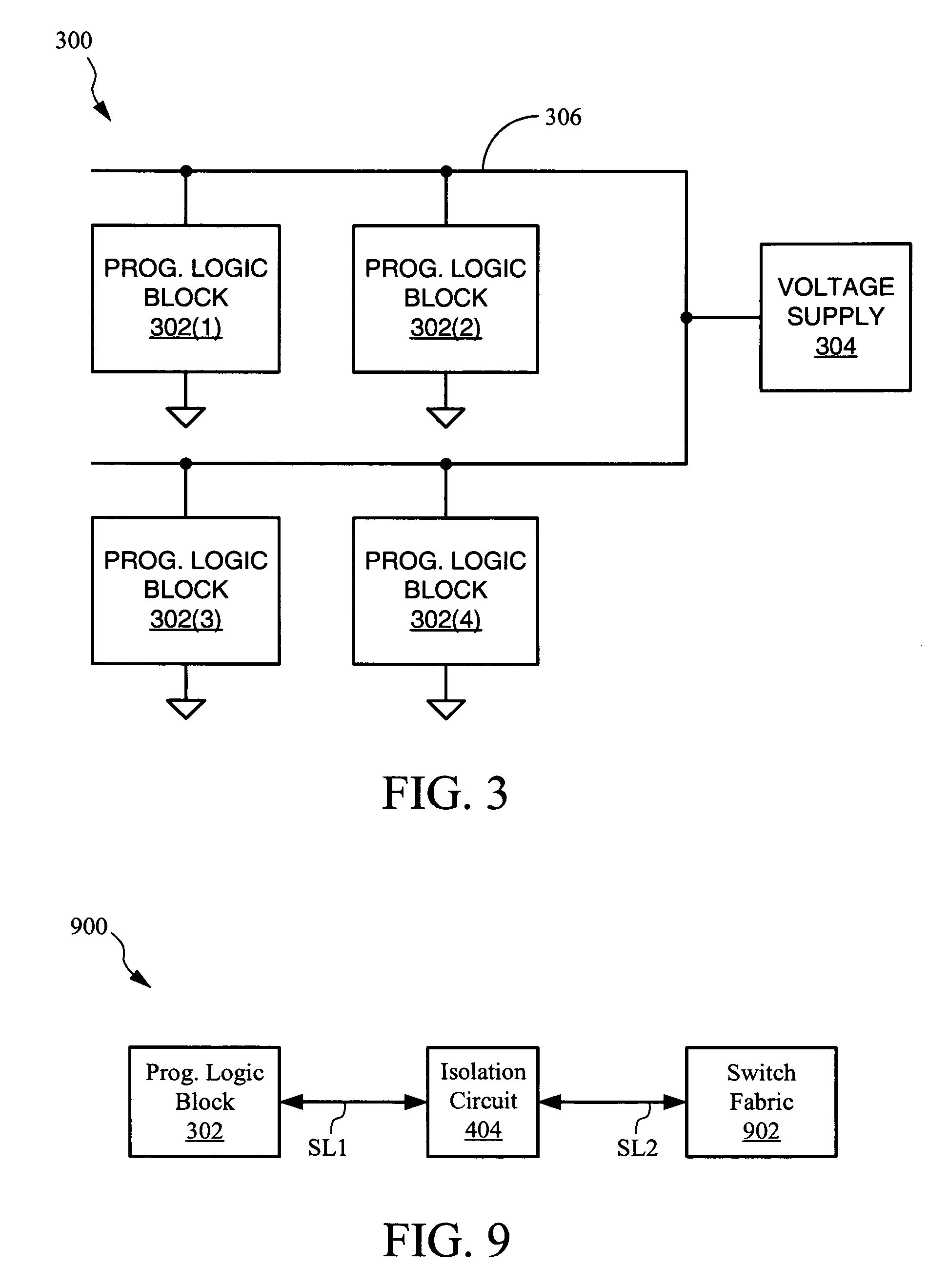
[0025]Embodiments of the present invention are described below in the context of an exemplary PLD architecture for simplicity only. It is to be understood that present embodiments are equally applicable to other PLD architectures such as FPGAs and complex PLDs, and to other types of integrated circuits including, for example, application-specific integrated circuit (ASIC) devices. In the following description, for purposes of explanation, specific nomenclature is set forth to provide a thorough understanding of the present invention. In other instances, well-known circuits and devices are shown in block diagram form to avoid obscuring the present invention unnecessarily. Further, the logic states of various signals described herein are exemplary and therefore may be reversed or otherwise modified as generally known in the art. Additionally, the interconnection between circuit elements or blocks may be shown as buses or as single signal lines. Each of the buses may alternatively be a...


PUM


Abstract

An integrated circuit device such as a PLD is divided into a plurality of logic blocks, each including one or more resources of the device. The device includes a plurality of switch elements and a number of signal isolation circuits. The switch elements selectively disable corresponding logic blocks to reduce power consumption, and the signal isolation circuits selectively isolates corresponding logic blocks to prevent the transmission of invalid data from disabled logic blocks to enabled logic blocks.

Description

CROSS-REFERENCE TO RELATED APPLICATIONS[0001]This application is related to co-pending and commonly-owned U.S. patent application Ser. No. 10 / 666,669 entitled “Disabling Unused / Inactive Resources In Programmable Logic Devices For Static Power Reduction” filed Sep. 19, 2003; U.S. patent application Ser. No. 10 / 783,216 entitled “Tuning Programmable Logic Devices For Low-Power Design Implementation” filed Feb. 20, 2004, and U.S. patent application Ser. No. 10 / 783,589 entitled “Regulating Unused / Inactive Resources In Programmable Logic Devices For Static Power Reduction” filed Feb. 20, 2004, all of which are incorporated herein by reference.FIELD OF INVENTION[0002]This invention relates generally to power supply distribution in integrated circuit (IC) devices, and in particular to selectively providing power to various portions of an IC device.DESCRIPTION OF RELATED ART[0003]A programmable logic device (PLD) is a general-purpose device that can be programmed by a user to implement a var...

Claims


Application Information

Patent Timeline
Patent Type & Authority Patents(United States)
IPC IPC(8): H03K19/177G06F7/38H01L25/00H01L29/73H03K19/173
CPCH03K19/17748H03K19/17784H01L27/11807
Inventor JENKINS, IV, JESSE H.
Owner XILINX INC
Why Eureka
Try Eureka