Supercharge Your Innovation With Domain-Expert AI Agents!

Method for testing an integrated circuit device having elements with asynchronous clocks or dissimilar design methodologies

a technology of integrated circuit devices and design methodologies, applied in the field of data processing systems and methods, can solve problems such as problems such as problems such as scanning across asynchronous clock boundaries, devices will require different clocking requirements, and cannot be used in systems-on-chip designs, and achieve the effect of reducing the design time and circuit area of the clock distribution design

Inactive Publication Date: 2009-03-03
INT BUSINESS MASCH CORP
View PDF14 Cites 18 Cited by
  • Summary
  • Abstract
  • Description
  • Claims
  • Application Information

AI Technical Summary

Benefits of technology

The patent describes a system and method for testing integrated circuits with asynchronous clocks or dissimilar design methodologies. The system eliminates the need for scanning across clock borders, reducing circuit area and design time. It uses dedicated scan chains for each clock domain and allows for separate testing of boundary logic in the asynchronous clock boundaries. The testing process involves inputting test pattern data to scan-in scan chains and capturing test output data at scan-out scan chains. The system also includes a boundary BIST for testing the proper operation of the boundary logic. Overall, the system and method provide a more efficient way to test complex integrated circuits.

Problems solved by technology

However, when input / output (I / O) and memory devices are incorporated on the same chip, these devices will require different clocking requirements.
Scanning across asynchronous clock boundaries is problematic because latch setup and hold times cannot be established reliably between the two clocking environments.
This is especially a problem when testing the operation of the microprocessor or SoC.
This, however, is not possible with microprocessors or systems-on-a chip designs that have different clocking domains on the chip.
Since they only need to run at 300 MHz functionally, this is not a very efficient design from a circuit area and power standpoint.

Method used


Image

  • Method for testing an integrated circuit device having elements with asynchronous clocks or dissimilar design methodologies
  • Method for testing an integrated circuit device having elements with asynchronous clocks or dissimilar design methodologies
  • Method for testing an integrated circuit device having elements with asynchronous clocks or dissimilar design methodologies

Examples


Embodiment Construction

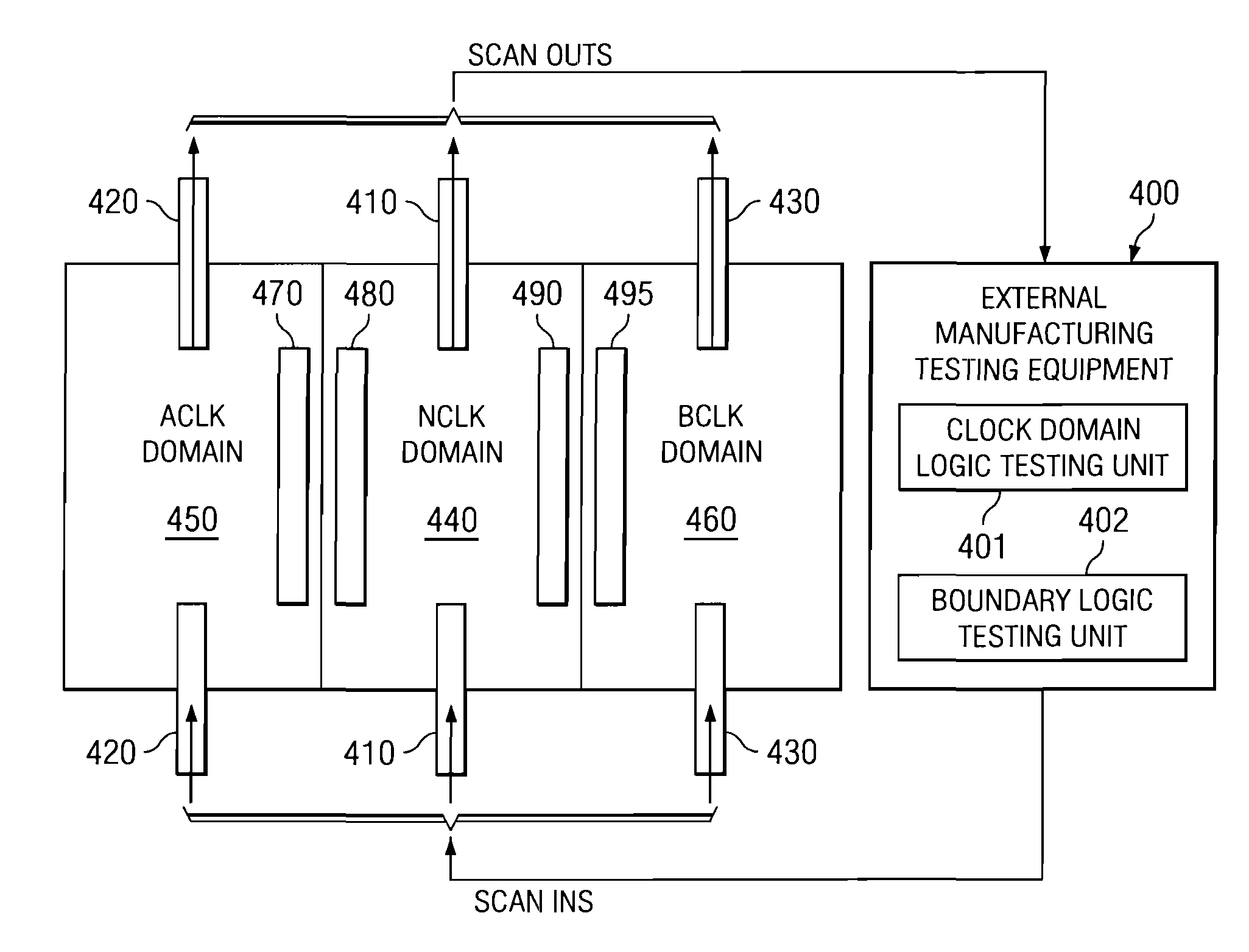
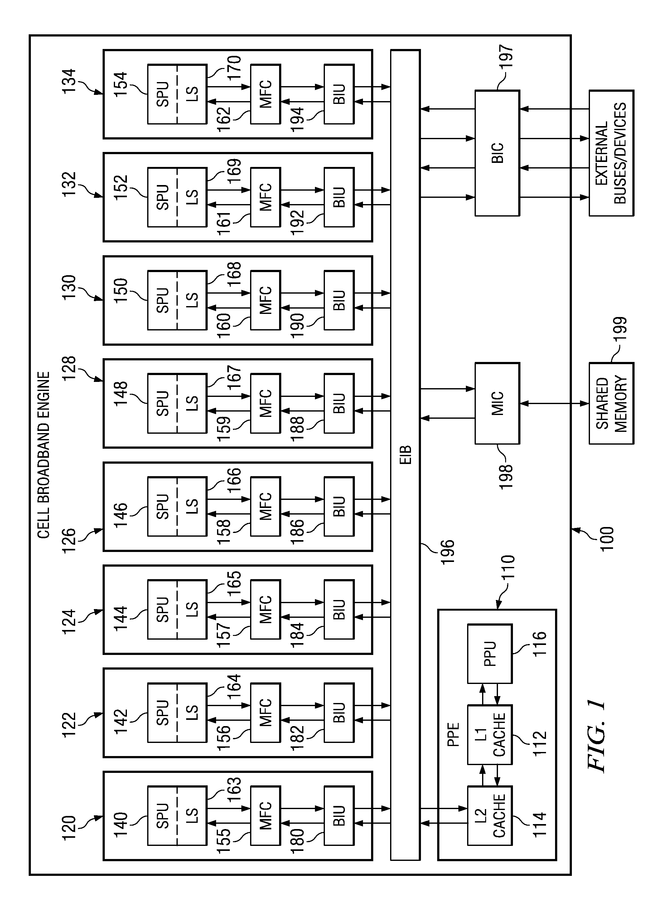
[0036]The illustrative embodiments provide a system and method for testing an integrated circuit device with asynchronous clocks or dissimilar design methodologies. As such, the illustrative embodiments may be utilized with any integrated circuit device in which there are different domains, e.g., a synchronous clock domain and an asynchronous clock domain, two different design methodology domains, or the like. In one illustrative embodiment, the mechanisms of the illustrative embodiments are implemented in a microprocessor chip or system-on-a-chip (SoC) and are utilized to test the proper functioning of the elements on the chip. In particular, in one illustrative embodiment the scan chains and boundary built-in-self-test (BIST) are applied to the Cell Broadband Engine (CBE) available from International Business Machines, Inc. of Armonk, N.Y. While the illustrative embodiments hereafter will be described with reference to the CBE, it should be appreciated that the present invention i...


PUM


Abstract

A method for testing an integrated circuit device with asynchronous clocks or dissimilar design methodologies is provided. With the method, each clock domain has its own scan paths that do not cross domain boundaries. By eliminating the scanning across the boundaries, the requirement to have two clock grids in the asynchronously clocked domains may be eliminated. As a result, circuit area and design time with regard to the clock distribution design are reduced. In addition, removing the second clock grid, i.e. the high speed core or system clock, in the asynchronously clocked domains removes the requirement to have a multiplexing scheme for selection of clocking signals in the asynchronous domain. In addition to the above, the method provides boundary built-in-self-test logic for testing the functional crossing logic of boundaries between the clock domains in a functional mode of operation.

Description

BACKGROUND[0001]1. Technical Field[0002]The present application relates generally to an improved data processing system and method. More specifically, the present application is directed to a system and method for testing an integrated circuit device with asynchronous clocks or dissimilar design methodologies.[0003]2. Description of Related Art[0004]When a microprocessor or system-on-a-chip (SoC) is designed, it is important that the resulting chip design be tested to ensure proper functioning. In order to test a microprocessor or SoC chip, typically, the chip is designed to include built-in scan chains for scanning in test patterns to individually test the cores and other circuitry elements of the microprocessor or SoC. A scan chain is formed by connecting a set of sequential elements, such as flip-flops or shift register latches, as a shift register chain in a processor or SoC design. Most modern processor or SoC chips have multiple scan chains to reduce testing application time a...

Claims


Application Information

Patent Timeline
Patent Type & Authority Patents(United States)
IPC IPC(8): G01R31/28
CPCG01R31/318552G01R31/318563G01R31/318594
Inventor CHELSTROM, NATHAN P.FERGUSON, STEVEN R.RILEY, MACK W.
Owner INT BUSINESS MASCH CORP
Features
  • R&D
  • Intellectual Property
  • Life Sciences
  • Materials
  • Tech Scout
  • Unparalleled Data Quality
  • Higher Quality Content
  • 60% Fewer Hallucinations
Learn More