Fabrication method of a wafer structure

a technology of oxidation resistance and fabrication method, which is applied in the direction of electrical equipment, semiconductor devices, semiconductor/solid-state device details, etc., can solve the problems of poor soldering of products and easy oxidation of the surface of high lead bumps, and achieve the effect of improving the quality of wafers

Active Publication Date: 2009-03-10
ADVANCED SEMICON ENG INC
View PDF11 Cites 23 Cited by
  • Summary
  • Abstract
  • Description
  • Claims
  • Application Information

AI Technical Summary

Benefits of technology

[0007]It is therefore the object of the invention to provide an oxidation-resistant wafer structure. Besides improving the quality of the wafer, the wafer structure according to the invention also avoids the cold-joint problem due to oxidation when the wafer structure is soldered to a substrate.

Problems solved by technology

However, the surface of the high lead bump is easily oxidized to form an oxide layer on the surface of the bump.
When the bump is bonded to an external component such as a substrate or a circuit board, the cold joint would easily occur, resulting in poor soldering of the product.

Method used


Image

  • Fabrication method of a wafer structure
  • Fabrication method of a wafer structure
  • Fabrication method of a wafer structure

Examples


first embodiment

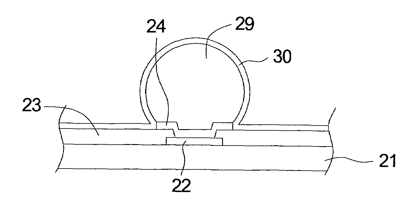
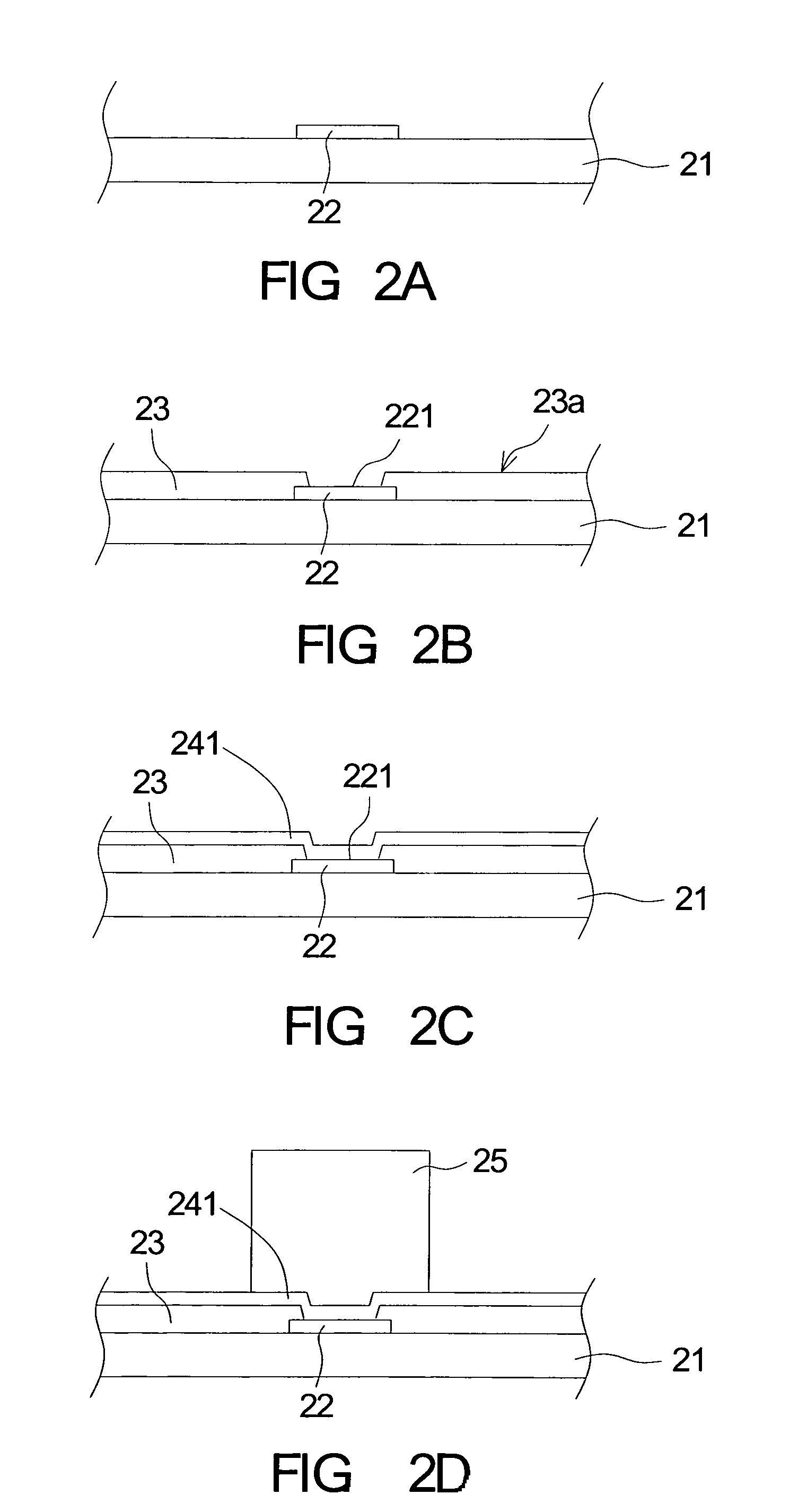
[0015]Referring to FIG. 2A˜2J, diagrams of a fabricating method of a flip-chip package according to a first embodiment of the invention are shown. At first, as shown in FIG. 2A, a wafer 21 is provided. The wafer 21 has a conductive structure such as a pad 22, normally made of copper or aluminum, disposed thereon to form an electrical connection with an external circuit. Next as shown in FIG. 2B, an organic protective layer 23 is applied on the wafer 21. The organic protective layer protects the wafer structure and flattens the surface. The organic protective layer 23 does not cover the entire pad 22 for a conductive surface 221 of the pad 22 to be exposed. Meanwhile, a wafer 21 having an active surface 23a is provided. The active surface 23a has several pads 22 disposed thereon.

[0016]Then, as shown in FIG. 2C, a conductive layer 241 is formed on the surface of the organic protective layer 23 and the pad 22 by using a sputtering method. Next, as shown in FIG. 2D, the conductive layer...

second embodiment

[0022]The invention is also applicable to a wafer structure having a copper bump and the flip-chip package structure thereof. The present embodiment differs with the above embodiment only in the material of the bump and the range covered by the organic protective layer, while the other components are the same. The wafer structure and the fabricating method thereof are exemplified below. The subsequent flip-chip package method still remains the same and is not illustrated in the present embodiment.

[0023]Referring to FIG. 3A˜3C, diagrams of a fabricating method of a wafer structure according to a second embodiment of the invention are shown. At first, a wafer 321 is provided. The active surface 323a of the wafer 321 has an organic protective layer 323 and a under bump metallurgy (UBM) layer 324. The bump of the UBM layer 324 is preferably a copper bump 329 formed on the UBM layer 324 as shown in FIG. 3A. The copper bump 329 is preferably a copper post which can be formed through the f...


PUM


Abstract

A wafer fabricating method at least includes the steps of providing a wafer having an active surface with a plurality of pads, forming a plurality of bumps on the pad, and forming an organic protective layer on the bump and the active surface. Besides improving the quality of the wafer, the wafer structure according to the invention is oxidation-resistant, thus avoiding the cold-joint problem when soldered to the substrate.

Description

[0001]This application claims the benefit of Taiwan application Serial No. 93133451, filed Nov. 3, 2004, the subject matter of which is incorporated herein by reference.BACKGROUND OF THE INVENTION[0002]1. Field of the Invention[0003]The invention relates in general to a fabricating method of a wafer structure, and more particularly to a fabricating method of an oxidation-resistant wafer structure.[0004]2. Description of the Related Art[0005]Referring to FIG. 1, cross-sectional view of a conventional wafer structure is shown. Conventional wafer structure 10 includes a wafer 11, a conductive structure, an organic protective layer 13, an under bump metallurgy layer (UBM layer) 14 and a conductive bump 15. The conductive structure, a pad 12 for example, is positioned on the surface of the wafer 11. The organic protective layer 13 covers the wafer 11 and part of the pad 12 to expose the surface of the pad 12. The UBM layer 14 is connected to the surface of the pad 12 to enhance the surfa...

Claims


Application Information

Patent Timeline
Patent Type & Authority Patents(United States)
IPC IPC(8): H01L21/00H01L21/60H01L23/48H01L23/485
CPCH01L24/11H01L24/13H01L2224/1147H01L2224/13099H01L2924/01013H01L2924/01022H01L2924/01029H01L2924/01042H01L2924/01074H01L2924/01075H01L2924/01078H01L2924/01082H01L2924/01005H01L2924/01006H01L2924/01023H01L2924/01024H01L2924/01033H01L2924/014H01L2224/13116H01L2224/13147H01L2224/136H01L2924/0105H01L2924/00014H01L2924/0001H01L24/03H01L24/05H01L2224/05001H01L2224/05022H01L2224/05124H01L2224/05147H01L2224/05155H01L2224/05166H01L2224/05171H01L2224/05184H01L2224/05572H01L2224/05647H01L2224/05669
Inventor TSAI, CHI-LONG
Owner ADVANCED SEMICON ENG INC
Why Eureka
Try Eureka