Method for improving wafer performance for photovoltaic devices
What is AI technical title?
AI technical title is built by PatSnap AI team. It summarizes the technical point description of the patent document.
a photovoltaic device and wafer technology, applied in the manufacture of final products, basic electric elements, sustainable buildings, etc., can solve the problems of reducing the performance of the wafer, and the difference between the quality of the wafer and so as to reduce the auto-generation of the hydrogen neutral charge-state fraction, and reduce the cost of the wafer
Active Publication Date: 2021-02-02
NEWSOUTH INNOVATIONS PTY LTD
View PDF2 Cites 0 Cited by
Summary
Abstract
Description
Claims
Application Information
AI Technical Summary
This helps you quickly interpret patents by identifying the three key elements:
Problems solved by technology
Method used
Benefits of technology
Benefits of technology
The patent describes a method for improving the quality of silicon wafers by using atomic hydrogen to passivate defects. By keeping the hydrogen atoms in a charged state, they are less likely to move away from imperfections. The method involves maintaining the temperature of the wafer at a given range to allow the atomic hydrogen to diffuse sufficiently quickly and avoid an excessive increase of thermal generation of the hydrogen neutral charge-state fraction. The method also includes controlling the injection levels by maintaining the temperature in a given range to minimize the auto-generation of the neutral charge-state of the hydrogen. Overall, this method allows for a higher quality silicon wafer.
Problems solved by technology
Electrically active defects throughout a PV cell affect the lifetime of charge carriers causing reduced performance.
These defects may be related to the quality of the wafer, or can be created during fabrication.
A significant trade-off exists between wafer cost and wafer quality.
Such wafers have a range of different types of crystallographic imperfections that degrade performance such as dislocations, grain boundaries and a range of other defects.
Wafer fabrication techniques that can reduce the density or severity of such crystallographic imperfections will add to the cost of the wafers, leading to the present range of commercially available wafers whereby the price is higher for wafers with a lower density and / or severity of crystallographic defects.
Method used
Image
Click on the blue label to locate the original text in one second.
Reading with bidirectional positioning of images and text.
Examples
Embodiment Construction
[0030]Embodiments of the present invention relate to the field of photovoltaics and processing of wafers, such as silicon wafers for manufacturing photovoltaic devices. In particular, embodiments relate to the incorporation of manufacturing processes to improve quality of silicon wafers and photovoltaic devices.
[0031]This disclosure is relevant to all crystalline and multi-crystalline silicon solar cells that capitalise on the hydrogen passivation of defects and / or recombination by diffusing or implanting or driving hydrogen into the defected regions of the silicon material and coupling some of this hydrogen preferentially to deep into the silicon material from one or more external hydrogen sources.
[0032]A silicon solar cell in the presence of one or more hydrogen sources that are able to thermally diffuse hydrogen into one or more of the surfaces of the silicon wafer that has crystallographic defects in the vicinity of the wafer surface. These defects preferably extend from the sur...
PUM
Property
Measurement
Unit
temperature
aaaaa
aaaaa
temperature
aaaaa
aaaaa
temperature
aaaaa
aaaaa
Abstract
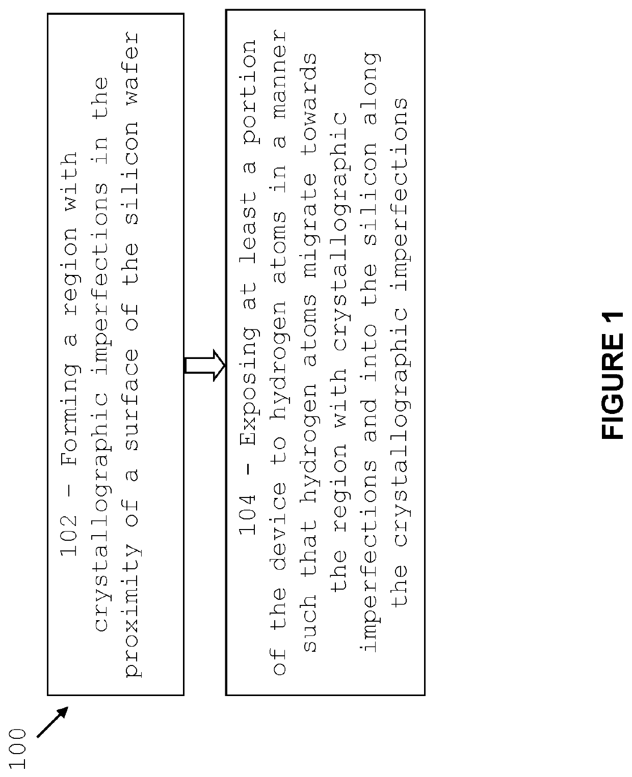
The present disclosure is directed to a method for processing a siliconwafer that allows improving performance by exploiting the properties of crystallographic imperfections. The method comprises the steps of: forming a silicon layer with crystallographic imperfections in the proximity of a surface of the silicon; exposing at least a portion of the device to hydrogen atoms in a manner such that hydrogen atoms migrate towards the region with crystallographic imperfections and into the silicon along the crystallographic imperfections; and controlling the charge state of hydrogen atoms located at the crystallographic imperfections to be positive when the imperfections are in a p-type region of the wafer; and negative when the imperfections are at an n-type region of the wafer by thermally treating the silicon while exposing the silicon to an illumination intensity of less than 10 mW / cm2.
Description
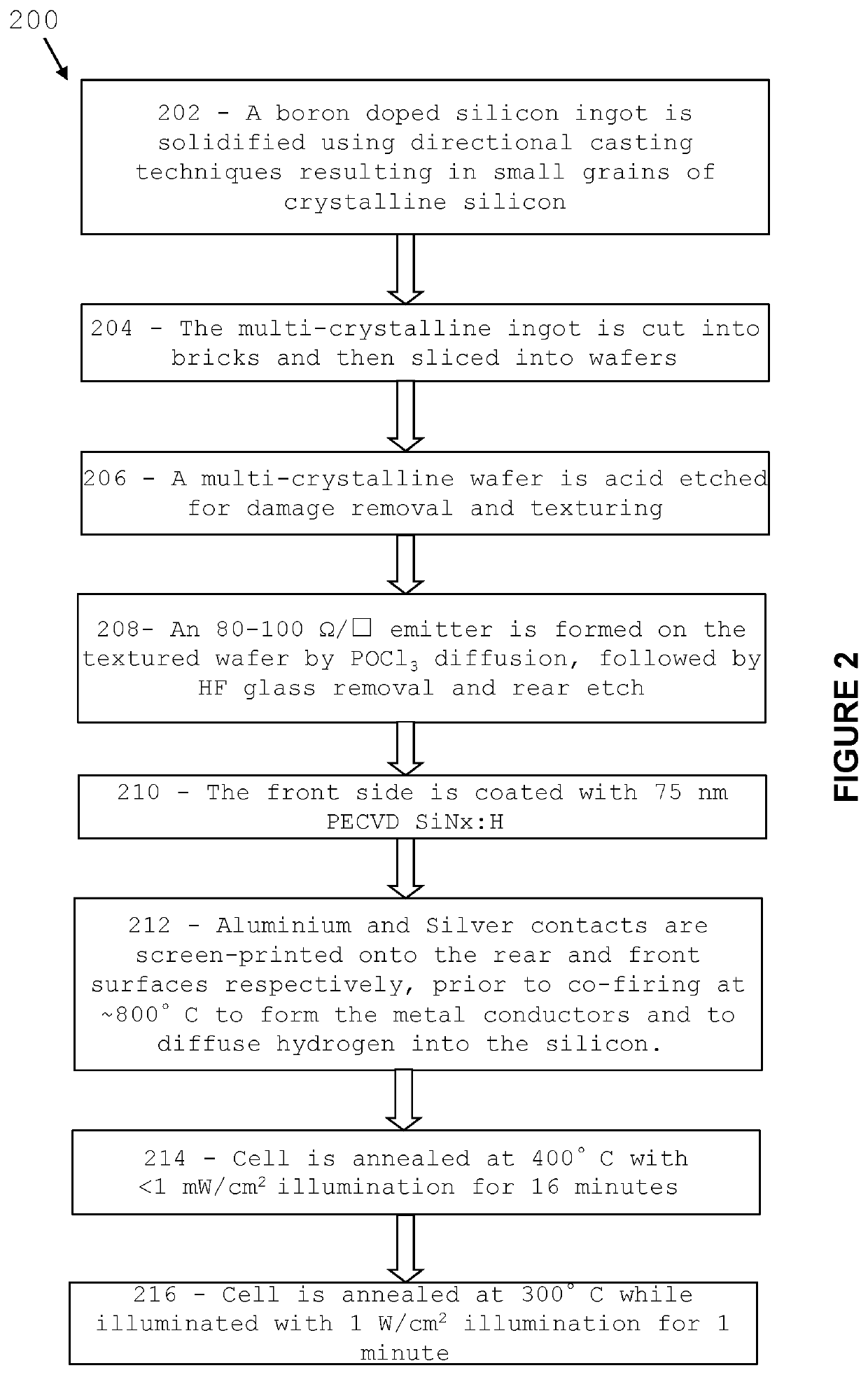
FIELD OF THE INVENTION[0001]The present invention generally relates to methods for manufacturing photovoltaic devices. In particular, the invention relates to manufacturing methods for improving the efficiency of photovoltaic devices.BACKGROUND OF THE INVENTION[0002]Silicon is the main semiconductor material used to fabricate today's commercial photovoltaic (PV) cells. The majority of commercial PV cells are fabricated from a monocrystalline or multi-crystalline silicon wafer. A p-n junction is formed in the silicon wafer by, for example, diffusing n-type atoms in a p-type silicon wafer.[0003]Electrically active defects throughout a PV cell affect the lifetime of charge carriers causing reduced performance. These defects may be related to the quality of the wafer, or can be created during fabrication.[0004]A significant trade-off exists between wafer cost and wafer quality. Currently, production is dominated by lower quality, lower cost multi-crystalline silicon wafers which achieve...
Claims
Application Information
Patent Timeline
Application Date:The date an application was filed.
Publication Date:The date a patent or application was officially published.
First Publication Date:The earliest publication date of a patent with the same application number.
Issue Date:Publication date of the patent grant document.
PCT Entry Date:The Entry date of PCT National Phase.
Estimated Expiry Date:The statutory expiry date of a patent right according to the Patent Law, and it is the longest term of protection that the patent right can achieve without the termination of the patent right due to other reasons(Term extension factor has been taken into account ).
Invalid Date:Actual expiry date is based on effective date or publication date of legal transaction data of invalid patent.

