Fabrication process of a semiconductor device

a technology of semiconductor devices and fabrication processes, which is applied in the direction of semiconductor devices, basic electric elements, electrical equipment, etc., can solve the problems of poor film quality and serious adhesion between the barrier metal film and the interlayer insulation film

Active Publication Date: 2009-03-24
FUJITSU LTD
View PDF6 Cites 22 Cited by
  • Summary
  • Abstract
  • Description
  • Claims
  • Application Information

AI Technical Summary

Problems solved by technology

However, such MOCVD process or ALD process generally uses metal organic vapor source, and because of this, the barrier metal film of refractory metal or refractory metal nitride formed with such a process suffers from the problem of poor film quality, in spite of its capability of forming a thin and uniform film.
For example, there arises a serious problem of adhesion between the barrier metal film and the interlayer insulation film particularly when a low-dielectric interlayer insulation film of low density, such as inorganic low-K film of SiOCH film or SiC film or organic insulation film, is used.

Method used


Image

  • Fabrication process of a semiconductor device
  • Fabrication process of a semiconductor device
  • Fabrication process of a semiconductor device

Examples


first embodiment

[0035]FIGS. 3A-3I show the fabrication process of a semiconductor device having a Cu interconnection structure according to a first embodiment of the present invention.

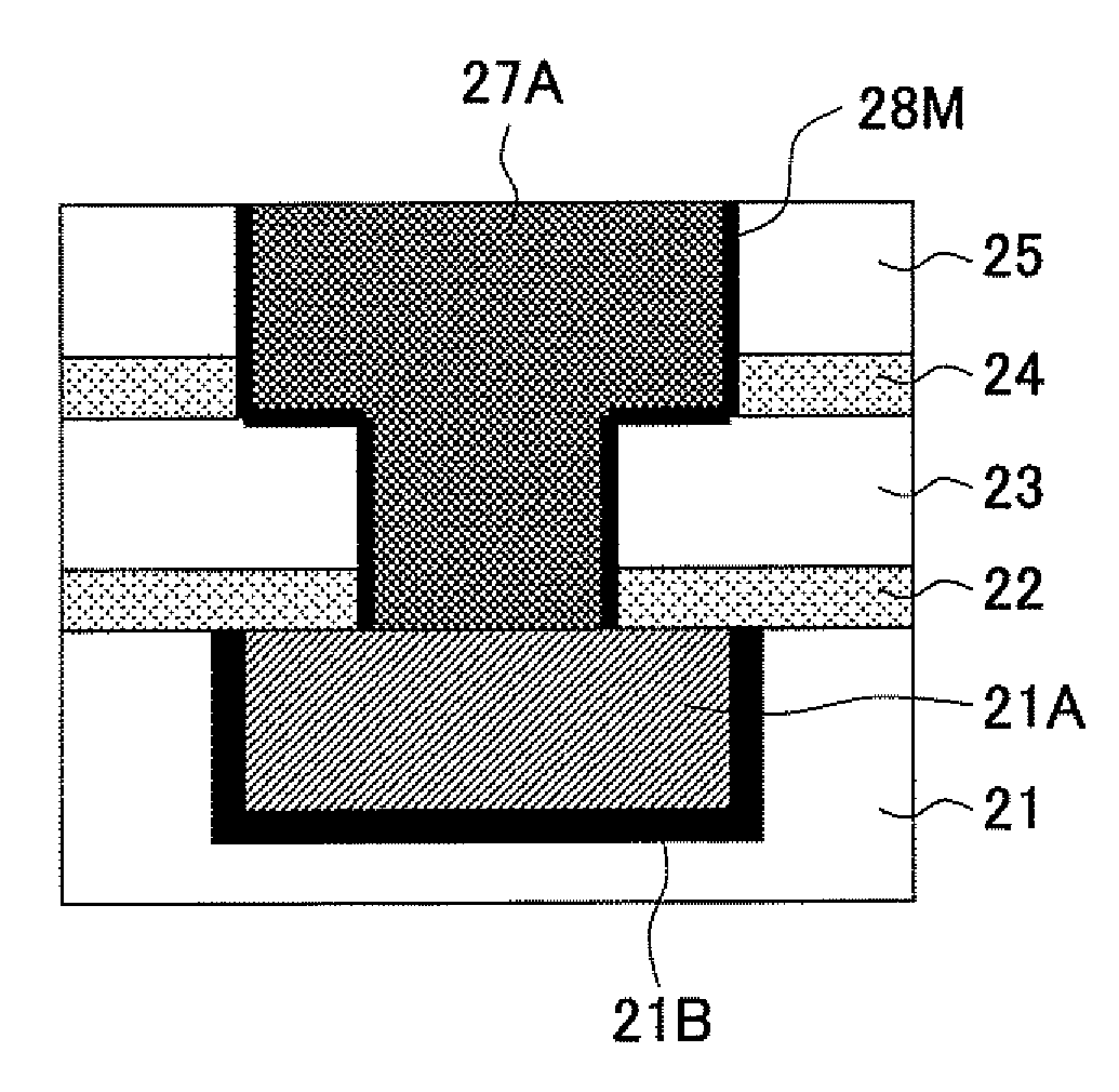
[0036]Referring to FIG. 3A, the semiconductor device of the present invention is a semiconductor device of the 45 nm node and includes an interlayer insulation film 21 formed on a substrate not illustrated, wherein a Cu interconnection pattern 21A of a width of 65 nm, for example, is embedded in the interlayer insulation film 21 via an ordinary barrier metal film 21B of Ta, TaN, or the like.

[0037]Further, on the interlayer insulation film 21, there are provided interlayer insulation films 23 and 25 each having a film thickness of 100-300 nm and formed by a plasma CVD process that uses TEOS for the source, via an etching stopper film 22 of SiC or SiN formed by a plasma CVD process with a film thickness of 10-50 nm, with an intervening etching stopper film 24 of SiC or SiN formed by a plasma CVD process with a thickness...

second embodiment

[0061]Next, the process of forming a Cu interconnection structure according to a second embodiment of the present invention will be described with reference to FIGS. 6A-6C. In the drawings, those parts explained before are designated by the same reference numerals and the description thereof will be omitted.

[0062]In the present embodiment, the Cu—Mn alloy layer 26 is formed in the first film forming apparatus (chamber 1) in the step of FIG. 6A corresponding to the first step of FIG. 3F, and the structure of FIG. 6A is transported to a second film forming apparatus (chamber 2) in the step of FIG. 6B through a high-vacuum environment of the pressure of 1×10⁻⁷ Pa or less together with the substrate (not shown) carrying the structure of FIG. 6A thereon while using a single-wafer processing apparatus equipped with a vacuum transportation chamber. There, the second step of the process of FIG. 3F is carried out. As a result, the Cu film 27a is formed on the Cu—Mn alloy layer 26.

[0063]Furth...

third embodiment

[0066]Next, the process of forming a Cu interconnection structure according to a third embodiment of the present invention will be described with reference to FIGS. 7A-7D. In the drawings, those parts explained before are designated by the same reference numerals and the description thereof will be omitted.

[0067]With the present embodiment, the Cu—Mn alloy layer 26 is formed in the step of FIG. 7A corresponding to the first step of FIG. 3F in the first film forming apparatus (chamber 1) and the surface of the Cu—Mn alloy layer 26 thus formed is exposed to the hydrogen radicals in the step of FIG. 7B in the same first film forming apparatus. With this, the surface of the Cu—Mn alloy layer 26 is terminated with hydrogen. The hydrogen radicals may be generated by forming hydrogen plasma. This hydrogen plasma processing may be conducted under the temperature of 100-150° C.

[0068]Meanwhile, there is a case that the low-K film constituting the interlayer insulation film is damaged as a res...


PUM

PropertyMeasurementUnit
pressureaaaaaaaaaa
thicknessaaaaaaaaaa
temperatureaaaaaaaaaa

Abstract

A method for fabricating a semiconductor device has forming an opening defined by an inner wall surface in an insulation film, covering said inner wall surface with a Cu—Mn alloy layer, depositing a first Cu layer over said Cu—Mn alloy layer without exposing said Cu—Mn alloy layer to the air, depositing a second Cu layer over said first Cu layer and filling said opening with said second Cu layer, and forming a barrier layer over said inner wall surface as a result of a reaction between Mn in said Cu—Mn alloy layer and said insulation film.

Description

CROSS-REFERENCE TO RELATED APPLICATION[0001]The present application is based on Japanese priority application No. 2006-307050 filed on Nov. 13, 2006, the entire contents of which are hereby incorporated by reference.BACKGROUND OF THE INVENTION[0002]The present invention generally relates to semiconductor devices and more particularly to a semiconductor device having a multilayer interconnection structure and fabrication process thereof.[0003]In recent semiconductor integrated circuit devices, a vast number of semiconductor elements are formed on a common substrate, and a multilayer connection structure is used for interconnecting these semiconductor elements.[0004]In multilayer interconnection structure, interlayer insulation films embedded with interconnection patterns constituting an interconnection layer are laminated, and a lower interconnection layer is connected to an upper interconnection layer by way of a via-contact formed in the interlayer insulation film.[0005]In the ultr...

Claims


Application Information

Patent Timeline
Patent Type & Authority Patents(United States)
IPC IPC(8): H01L21/4763
CPCH01L21/76814H01L21/76831H01L21/76843H01L21/76861H01L21/76862H01L21/76864H01L21/76873H01L2221/1089
Inventor OHTSUKA, NOBUYUKISHIMIZU, NORIYOSHINAKAO, YOSHIYUKI
Owner FUJITSU LTD
Why Eureka
Try Eureka