Design method and architecture for power gate switch placement and interconnection using tapless libraries

a technology of tapless libraries and design methods, applied in the direction of cad circuit design, pulse technique, instruments, etc., can solve the problem of incurred silicon area costs in providing the third rail, and achieve the effect of less routing resources and higher circuit densities

Active Publication Date: 2009-03-24
ANSYS
View PDF1 Cites 30 Cited by
  • Summary
  • Abstract
  • Description
  • Claims
  • Application Information

AI Technical Summary

Problems solved by technology

Leakage currents flow in logic circuits from a power supply node into the ground node because the switching characteristics of the transistors in the logic circuits are not ideal (i.e., the transistors cannot be completely shut off).
A considerable silicon area cost is therefore incurred in providing the third rail.

Method used


Image

  • Design method and architecture for power gate switch placement and interconnection using tapless libraries
  • Design method and architecture for power gate switch placement and interconnection using tapless libraries
  • Design method and architecture for power gate switch placement and interconnection using tapless libraries

Examples


Embodiment Construction

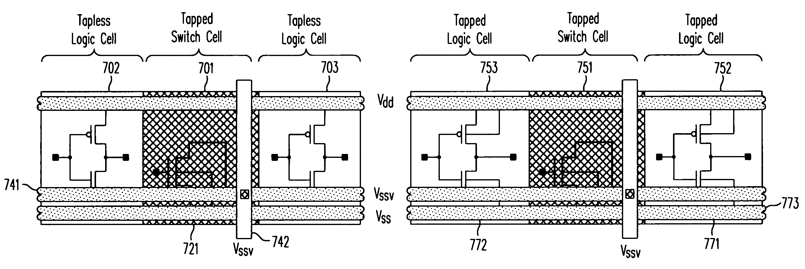
[0027]The present invention is applicable to integrated circuits designed using a “tapless” library. In a tapless library, the transistors in a standard cell are not provided within the standard cell the conventional tap connections to their appropriate P-well or N-well (“substrate”), so as to reduce the area requirement. Instead, a well tap is provided in the switch cells to connect the substrate with the appropriate ground or power supply reference. In an integrated circuit built from a tapless library, switch cells are placed among the standard cells at regular or approximately regular intervals, or within a selected distance (e.g., 50 microns), so that the standard cells that share a substrate with a switch cell may share the switch cell's low resistance substrate connection to the power supply or ground reference.

[0028]FIG. 7, which is subdivided into FIGS. 7a and 7b, illustrates the advantages of using tapless standard cells power-gated by switch cells to form an integrated ci...


PUM


Abstract

A method and a structure provide a space efficient integrated circuit using standard cells and power gating by switch cells. The standard cells may be tapless, i.e., not provided a substrate connection to a power supply or ground rail by a tap within the cell. The substrate connection for these standard cells may be provided by the switch cells or by specialized tap cells. The tapless standard cells may include only a context-sensitive rail, which may be configured to be a virtual ground rail by a power gating connection to a switch cell or by a direct connection to a power supply or ground rail.

Description

BACKGROUND OF THE INVENTION[0001]1. Field of the Invention[0002]The present invention relates to a method for designing multi-threshold complementary metal-oxide-semiconductor (MTCMOS) circuits and the physical architecture of the circuits resulting from using such a method. In particular, the present invention relates to a design method for providing power gating in an MTCMOS circuit using standard cells that provide a “context-sensitive” conductive traces, and the physical circuit architecture of MTCMOS circuits resulting from using this method.[0003]2. Discussion of the Related Art[0004]A significant concern in integrated circuit design is reducing leakage currents. Leakage currents flow in logic circuits from a power supply node into the ground node because the switching characteristics of the transistors in the logic circuits are not ideal (i.e., the transistors cannot be completely shut off).[0005]In MTCMOS circuits, one technique that reduces leakage current is to a place a “...

Claims


Application Information

Patent Timeline
Patent Type & Authority Patents(United States)
IPC IPC(8): G06F17/50H03K19/20
CPCG06F17/5068G06F2217/78G06F30/39G06F2119/06
Inventor FRENKIL, GERALD L.
Owner ANSYS
Why Eureka
Try Eureka