Photo-electric converting device and its driving method, and its manufacturing method, solid-state image pickup device and its driving method and its manufacturing method

a technology of photoelectric converting and driving method, which is applied in the direction of radio frequency controlled devices, television system scanning details, etc., can solve the problems of reducing the amount of light incident on unable to obtain sufficient sensitivity of the photo-electric converting portion b>53/b>, etc., and achieve suppression of an increase of dark current and high sensitivity characteristics

Active Publication Date: 2009-03-31
SONY SEMICON SOLUTIONS CORP
View PDF8 Cites 63 Cited by
  • Summary
  • Abstract
  • Description
  • Claims
  • Application Information

AI Technical Summary

Benefits of technology

[0030]It is another object of the present invention to provide a solid-state image pickup device, its driving method and its manufacturing method in which a high sensitivity characteristic and suppression of an increase of a dark current caused by interface states can be achieved at the same time.

Problems solved by technology

As a consequence, the amount of light that becomes incident on the photo-electric converting portion 53 decreases finally, and a problem arises, in which the photo-electric converting portion 53 cannot obtain sufficient sensitivity.

Method used


Image

  • Photo-electric converting device and its driving method, and its manufacturing method, solid-state image pickup device and its driving method and its manufacturing method
  • Photo-electric converting device and its driving method, and its manufacturing method, solid-state image pickup device and its driving method and its manufacturing method
  • Photo-electric converting device and its driving method, and its manufacturing method, solid-state image pickup device and its driving method and its manufacturing method

Examples


Embodiment Construction

[0058]The present invention will be described below with reference to the drawings.

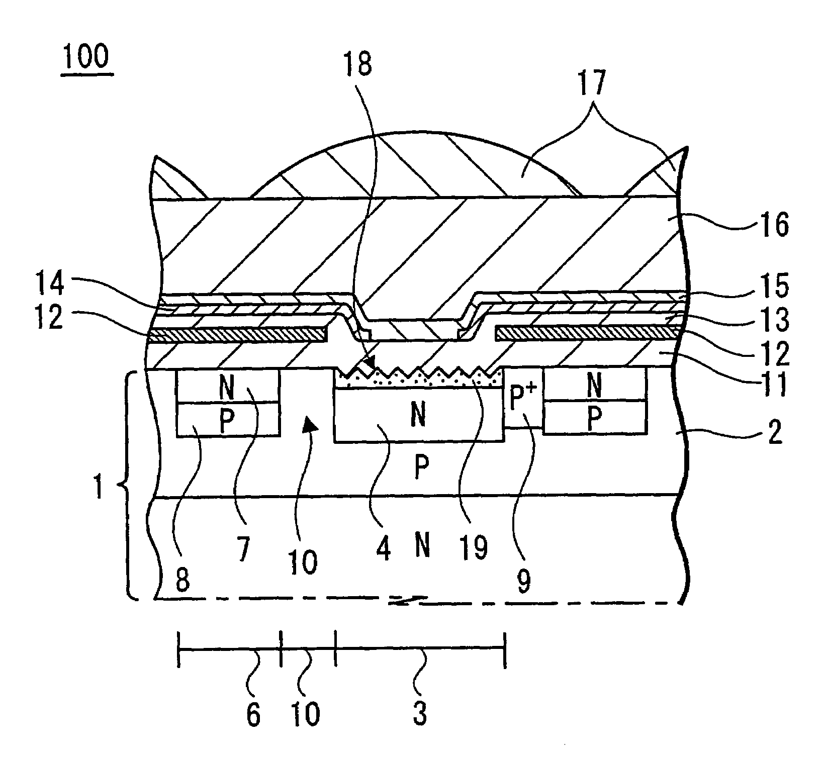
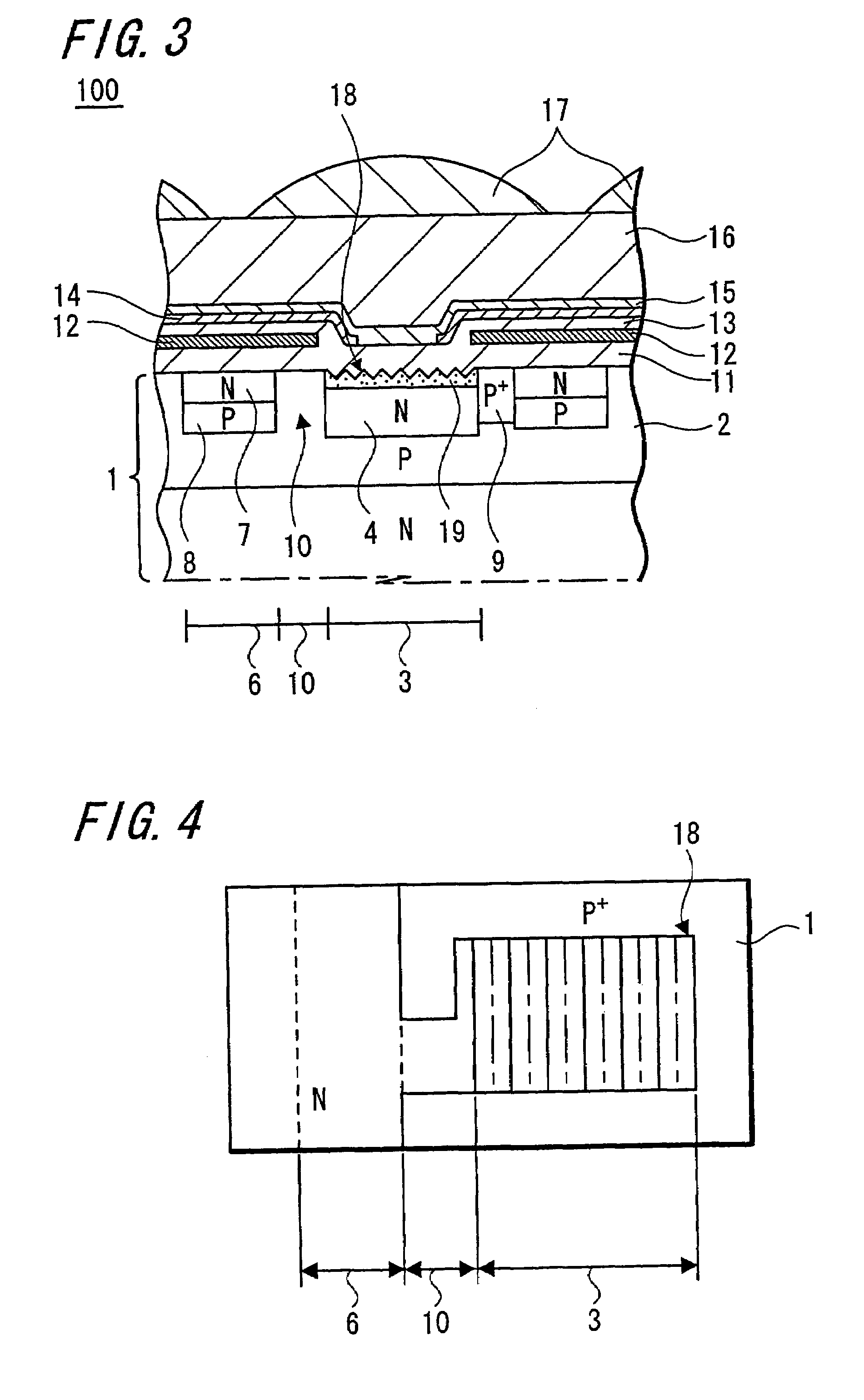
[0059]First, a solid-state image pickup device according to an embodiment of the present invention will be described with reference to FIG. 3 which is an enlarged cross-sectional view.

[0060]As shown in FIG. 3, a solid-state image pickup device 100 according to this embodiment includes an N-type silicon semiconductor substrate 1 which is mainly made of high-purity single crystal silicon (Si) in which a P-type first semiconductor well layer 2 is formed. A photo-diode formed of an N-type semiconductor region (so-called electric charge accumulating region) 4, for example, comprising a photo-electric converting portion 3 is formed on the surface side of the semiconductor substrate 1.

[0061]An N-type transfer channel region 7 comprising a vertical CCD portion 6 is formed on one side of the row of the photo-electric converting portion 3, and a P-type second semiconductor well region 8 is formed under the N-ty...


PUM


Abstract

A photo-electric converting apparatus 100 has an arrangement in which a photo-electric converting apparatus 3 is formed on the surface of a substrate 1, an insulating film 11 is formed on the substrate 1, an uneven portion 18 having concavities and convexities in the thickness direction of the substrate 1 is formed on at least a part of the interface between the substrate 1 of the photo-electric converting portion and the insulating film 11 and a recombination region 19 for decreasing a dark current is formed so as to contain the uneven portion 18 within the photo-electric converting portion 3. This photo-electric converting apparatus becomes able to obtain a high sensitivity characteristic and to suppress a dark current from being increased by a decrease of the interface states.

Description

BACKGROUND OF THE INVENTION[0001]1. Field of the Invention[0002]The present invention relates to a photo-electric converting device and its driving method, and its manufacturing method. Also, the present invention relates to a solid-state image pickup device, and its driving method and its manufacturing method.[0003]2. Description of the Related Art[0004]A solid-state image pickup device, for example, an ordinary solid-state image pickup device includes a plurality of photo-electric converting portions like photo-diodes arrayed as light-receiving cells in a one-dimensional fashion (linearly) or in a two-dimensional fashion (in a matrix fashion) on the surface of a semiconductor substrate. When light becomes incident on each of these photo-electric converting portions, signal charges are generated in response to the light and those signal charges are read out by a transfer electrode as a video signal.[0005]FIG. 1 of the accompanying drawings is a cross-sectional view showing a solid-...

Claims


Application Information

Patent Timeline
Patent Type & Authority Patents(United States)
IPC IPC(8): H04N3/14H04N5/335H01L21/76H01L27/14H01L27/146H01L27/148H01L29/74H01L29/768H01L31/0352H01L31/10H04N5/359H04N5/361H04N5/369H04N5/3725
CPCH01L27/1462H01L27/14627H01L27/14687H01L31/0352H01L27/14806H01L27/1485H01L27/14689H01L27/14812H01L27/146H01L31/10
Inventor MURAKAMI, ICHIRO
Owner SONY SEMICON SOLUTIONS CORP
Why Eureka
Try Eureka