Semiconductor device and method of manufacturing semiconductor device

a semiconductor and semiconductor technology, applied in semiconductor devices, capacitors, electrical devices, etc., can solve problems such as leakage current increase, and achieve the effect of suppressing the increase in leakage current increasing the capacitance of the capacitive elemen

Inactive Publication Date: 2013-02-05
RENESAS ELECTRONICS CORP
View PDF7 Cites 2 Cited by
  • Summary
  • Abstract
  • Description
  • Claims
  • Application Information

AI Technical Summary

Benefits of technology

[0013]According to the invention, the lower electrode including a metal includes an oxide layer having a thickness of 2 nm or less on the surface layer. In this case, the dielectric film includes a first phase appearing at room temperature in the bulk state and a second phase appearing at a higher temperature than that in the first phase in the bulk state. The second phase has a higher relative permittivity than that of the first phase. For this reason, even when the thickness of the dielectric film is not reduced, it is possible to increase the capacitance of the capacitive element. In addition, since it is not necessary to reduce the thickness of the dielectric film more than necessary, it is possible to suppress the increase in the leakage current of the capacitive element.
[0016]According to the invention, it is possible to increase the capacitance of the capacitive element without increasing the planar shape thereof, and to suppress the increase in the leakage current of the capacitive element.

Problems solved by technology

However, when the thickness of the capacitive dielectric film is excessively reduced, the leakage current increases.

Method used


Image

  • Semiconductor device and method of manufacturing semiconductor device
  • Semiconductor device and method of manufacturing semiconductor device
  • Semiconductor device and method of manufacturing semiconductor device

Examples


Embodiment Construction

[0028]The invention will be now described herein with reference to illustrative embodiments. Those skilled in the art will recognize that many alternative embodiments can be accomplished using the teachings of the present invention and that the invention is not limited to the embodiments illustrated for explanatory purposes.

[0029]Hereinafter, the embodiment of the invention will be described with reference to the accompanying drawings. In all the drawings, like elements are referenced by like reference numerals and descriptions thereof will not be repeated.

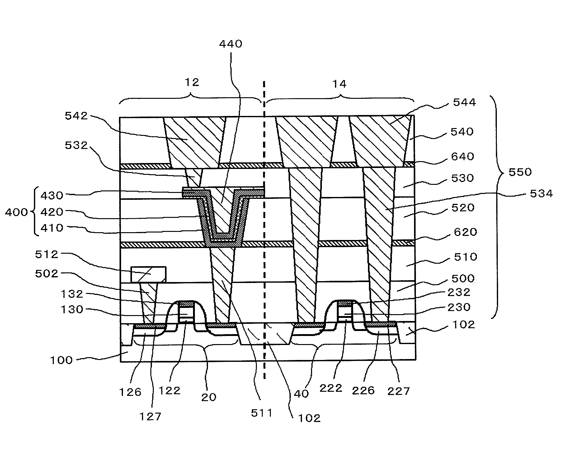
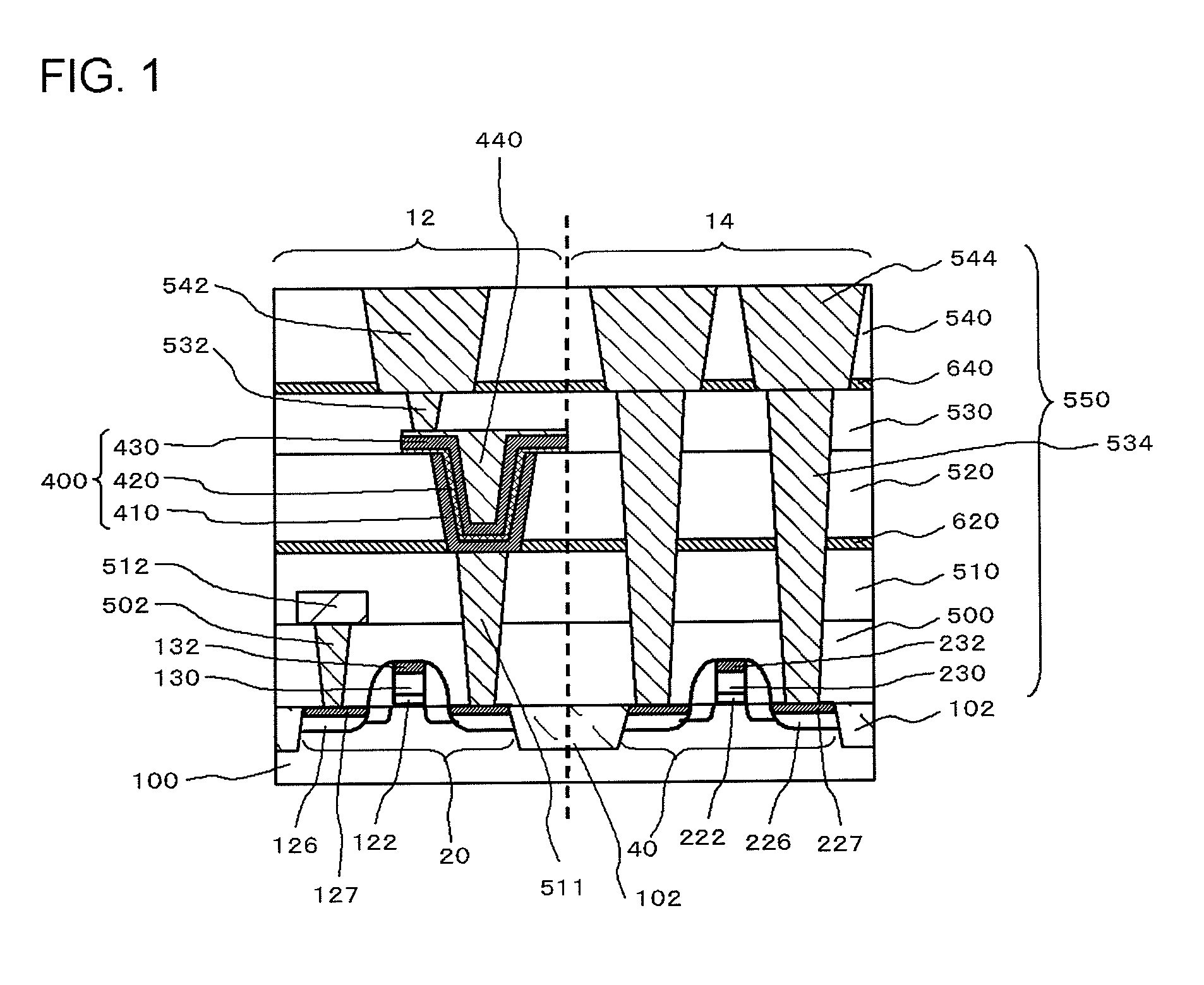
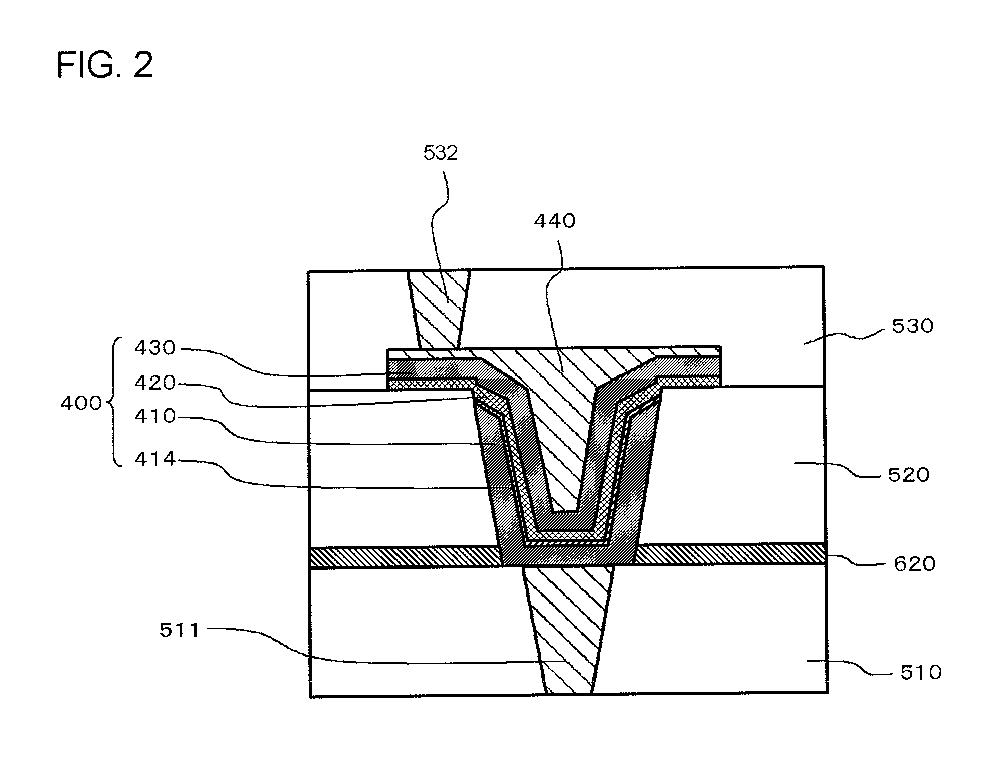
[0030]FIG. 1 is a cross-sectional view illustrating the configuration of a semiconductor device according to an embodiment. FIG. 2 is a cross-sectional view illustrating the configuration of a capacitive element 400 shown in FIG. 1. This semiconductor device includes a substrate 100, a transistor 40, a multilayer interconnect layer 550, and a capacitive element 400. The substrate 100 is a semiconductor substrate made of silicon an...


PUM

PropertyMeasurementUnit
thicknessaaaaaaaaaa
thicknessaaaaaaaaaa
temperatureaaaaaaaaaa

Abstract

A lower electrode includes a metal-containing oxide layer having a thickness of 2 nm or less on the surface layer. A metal-containing oxide layer is formed by oxidizing the surface of the lower electrode. A dielectric film includes a first phase appearing at room temperature in the bulk state and a second phase appearing at a higher temperature than that in the first phase in the bulk state. The second phase has a higher relative permittivity than that of the first phase.

Description

[0001]The application is based on Japanese patent application No. 2010-133356, the content of which is incorporated herein by reference.BACKGROUND[0002]1. Technical Field[0003]The present invention relates to a semiconductor device including a capacitive element and a method of manufacturing the semiconductor device.[0004]2. Related Art[0005]Capacitive elements are often incorporated in semiconductor devices. Since miniaturization of semiconductor devices has progressed in recent years, it has become necessary to increase the capacitance of the capacitive element without increasing the planar shape thereof. For example, Japanese Unexamined Patent Publication No. 2008-288408 and Japanese Unexamined Patent Publication No. 2007-158222 disclose that the capacitive element is formed in a three-dimensional type in order to increase the capacitance of the capacitive element.[0006]In addition, in order to increase the capacitance of the capacitive element without increasing the area thereof...

Claims


Application Information

Patent Timeline
Patent Type & Authority Patents(United States)
IPC IPC(8): H01L29/00
CPCH01L21/02244H01L21/02252H01L21/02356H01L28/91H01L27/10894H01L28/40H01L27/10852H10B12/09H10B12/033
Inventor IWAKI, TAKAYUKIITOU, TAKAMASASHIMIZU, KANA
Owner RENESAS ELECTRONICS CORP
Why Eureka
Try Eureka