Semiconductor memory device

a memory device and semiconductor technology, applied in the direction of information storage, static storage, digital storage, etc., can solve the problems of reducing reliability, hardly speeding up erasing action, and substantially taking 300 milliseconds to apply the pulsed erase voltage at step sb>3/b>, so as to minimize the overall writing time and the effect of tim

Inactive Publication Date: 2009-03-31
SHARP KK
View PDF6 Cites 50 Cited by
  • Summary
  • Abstract
  • Description
  • Claims
  • Application Information

AI Technical Summary

Benefits of technology

[0027]The present invention has been developed in view of the above aspects and its object is to provide a semiconductor memory device which can write the data in an array of memory cells including variable resistor elements rapidly and certainly as is higher in the freedom of functioning.

Problems solved by technology

Furthermore, the application of the pulsed erase voltage at Step S3 takes substantially 300 milliseconds.
When the source voltage is increased, the tunnel current between bands will be large enough to trap the holes in the tunnel oxide layer thus declining the reliability.
Since the increase of the source voltage is unfavorable, the erasing action will hardly be speeded up.
The conventional types of flash memory however have a drawback that the action of writing the data consumes a considerable length of time and remains limited in the data size to be handled.
Also, another drawback is to spare an extra storage area for buffering files, hence making the action of writing the data extremely complicated in steps.
Accordingly, even when the algorithm for writing employed in the conventional flash memory is applied to the resistive nonvolatile memory including the variable resistor element, the speeding up expected for each memory cell will not necessarily be expected in the whole device.

Method used


Image

  • Semiconductor memory device
  • Semiconductor memory device
  • Semiconductor memory device

Examples


first embodiment

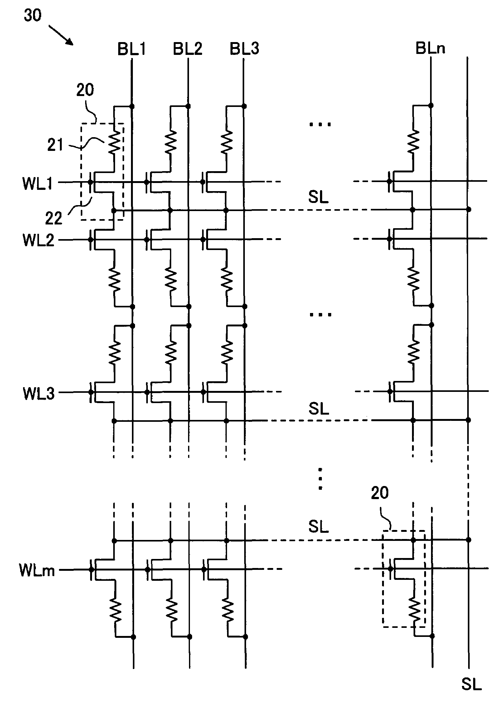
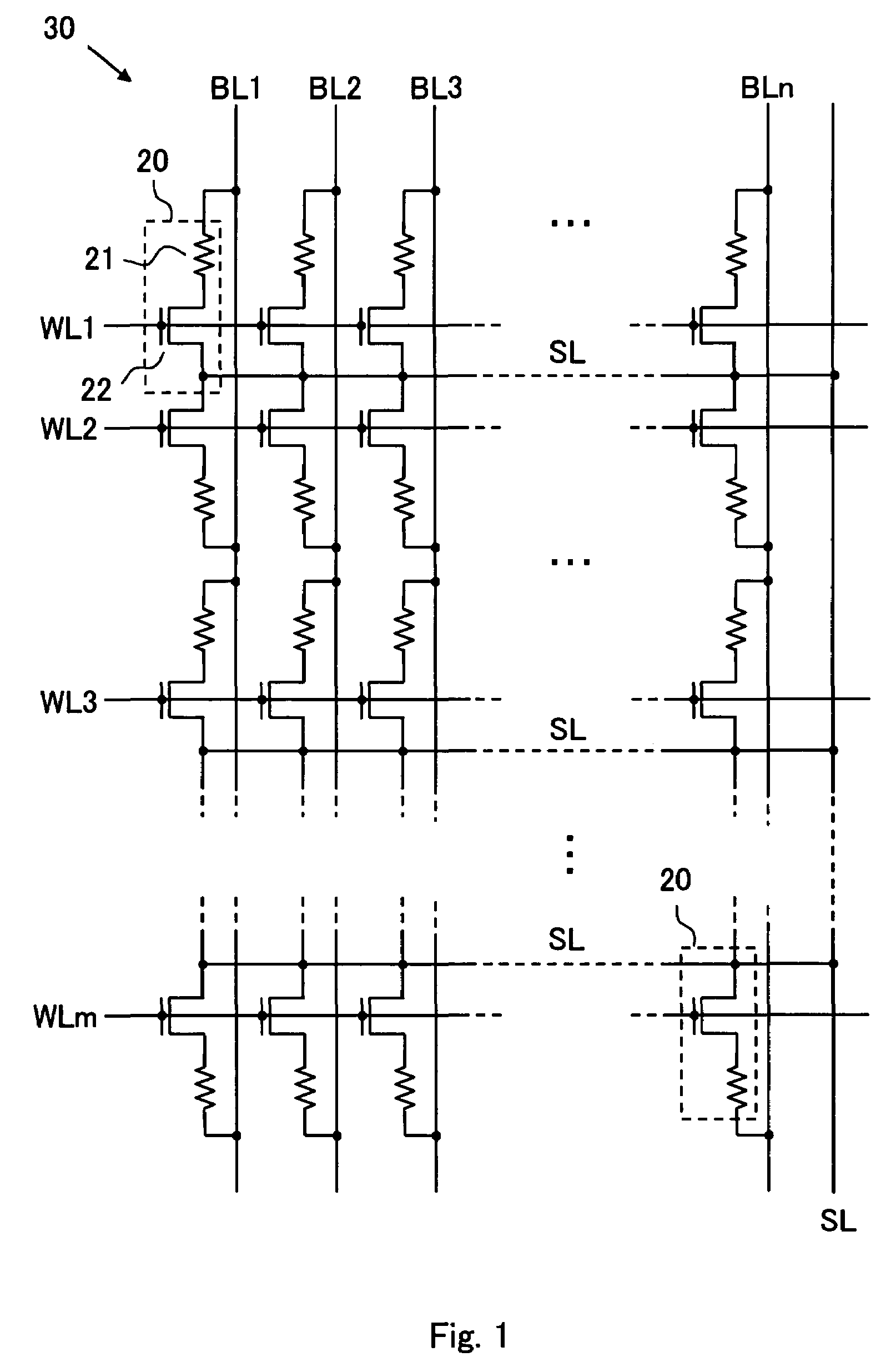
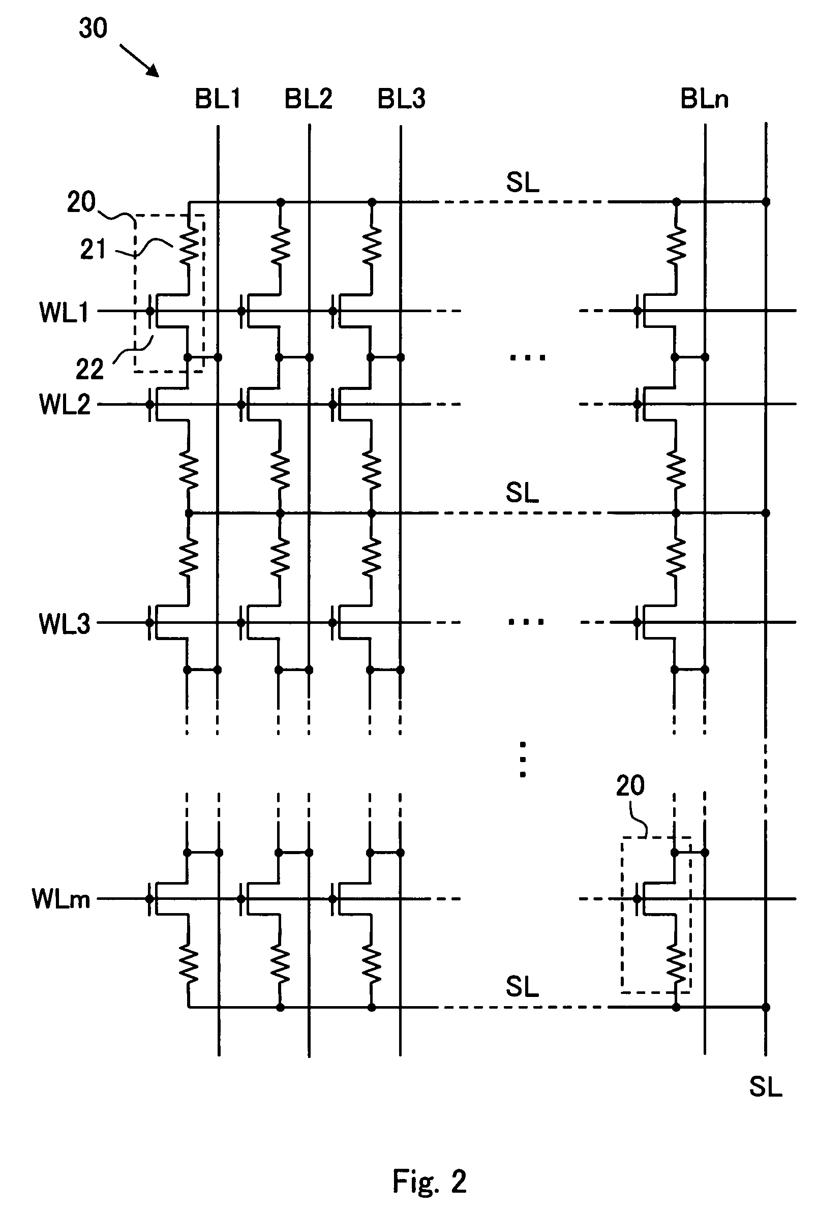
[0064]The inventive device comprises one or more memory cell arrays 30, each memory cell array having an array of memory cells 20 arranged in rows and columns, an m number of word lines WL1 to WLm arranged along the rows and an n number of bit lines BL1 to BLn arranged along the columns for selecting one or more memory cells, and a number of source lines SL arranged along the rows, as shown in FIG. 1. The source lines SL shown in FIG. 1 extend in parallel with the word lines WL1 to WLm along the rows and are connected at one end to a common line at the outside of the memory cell array 30. Alternatively, each source line SL may be accompanied with two adjacent word lines WL or arranged to extend along the columns but not the rows. Moreover, the source lines SL may be provided separately in the memory cell array 30 and arranged for selecting one or more memory cells in conjunction with the word lines and the bit lines.

[0065]The memory cell array 30 is not limited to the arrangement of...

second embodiment

[0103]The second embodiment of the present invention will now be described. In the above first embodiment, assuming that the variable resistor element 21 of the memory cell 20 in the memory cell array 30 shown in FIG. 1 is arranged to have the writing profile shown in FIG. 5 and the writing time profile shown in FIG. 6, the requirements for applying voltage are described about the cases where some or entire of the memory cells in the memory cell array 30 are subjected at once to the erasing action and where the memory cells in the memory cell array 30 are subjected one by one to the programming action. This embodiment is different from the first embodiment in the requirements for applying voltage since both the writing profile and the writing time profile are not equal to those of the first embodiment.

[0104]It is now assumed that the memory cell array, its peripheral circuits, and the writing profile (the relationship between the polarity of the applying voltage and a change in the ...

third embodiment

[0116]The third embodiment of the present invention will be described. As described previously, the writing action of the first embodiment involves erasing at once all the memory cells to be written or repeatedly erasing at once some of the memory cells to be written, and subjecting desired ones of the erased memory cells to the programming action. However, the storage state (the resistance state of the variable resistor element) is not always uniform before the action of erasing at once the memory cells to be written. When the voltage is applied to the variable resistor elements which are different in the resistance state at the initial stage under the same condition for the erasing action, they may be varied in the erased state (at the first state of the electric resistance). Accordingly, when subjected to the programming action, the variable resistor elements will furthermore be varied in the programmed state (at the second state of the electrical resistance), hence possibly inte...


PUM


Abstract

A semiconductor memory device comprises a array of memory cells arranged in a matrix, each memory cell connected to one end of a variable resistor element where the electric resistance is shifted from the first state to the second state by applying the first writing voltage and from the second state to the first state by applying the second writing voltage, and the source or drain of the selecting transistor. The second writing time for the second writing action of shifting the electric resistance of the variable resistor element from the second state to the first state is longer than the first writing time of shifting the same reversely. The second number of the memory cells subjected to the second writing action at once is greater than the first memory cell number subjected to the first writing action at once, and at least the second number is two or more.

Description

CROSS REFERENCE TO RELATED APPLICATION[0001]This Nonprovisional application claims priority under 35 U.S.C. §119(a) on Patent Application No. 2006-138592 filed in Japan on 18 May, 2006, the entire contents of which are hereby incorporated by reference.BACKGROUND OF THE INVENTION[0002]1. Field of the Invention[0003]The present invention relates to a semiconductor memory device which has an array of memory cells arranged in rows and columns, each memory cell comprising a variable resistor element accompanied with a selecting transistor for storing a data by changing its electrical resistance in response to application of a voltage.[0004]2. Description of the Related Art[0005]Such a nonvolatile semiconductor memory device, namely a flash memory, has widely been utilized as a small-sized, mass data recording medium in a wide range of applications including a computer, a communications apparatus, a measuring apparatus, an automated control apparatus, and a house-hold or personal applianc...

Claims


Application Information

Patent Timeline
Patent Type & Authority Patents(United States)
IPC IPC(8): G11C11/00
CPCG11C11/16G11C13/0007G11C13/0061G11C13/0069G11C2213/31G11C2213/79
Inventor HORII, SHINJISATO, SHINICHIYAMAGATA, SATORU
Owner SHARP KK
Why Eureka
Try Eureka