Internal reference voltage generating circuit for reducing standby current and semiconductor memory device including the same

a reference voltage generation circuit and standby current technology, applied in the direction of digital storage, instruments, reliability increasing modifications, etc., can solve the problem of increasing the power consumption of the semiconductor memory device b>100, and achieve the effect of reducing the number of pins

Inactive Publication Date: 2009-04-07
SAMSUNG ELECTRONICS CO LTD
View PDF7 Cites 30 Cited by
  • Summary
  • Abstract
  • Description
  • Claims
  • Application Information

AI Technical Summary

Benefits of technology

[0010]Exemplary embodiments of the present invention provide an internal reference voltage generating circuit that reduces a standby current and reduces the number of pins of a semiconductor memory device.
[0011]Exemplary embodiments of the present invention provide a semiconductor memory device including an internal reference voltage generating circuit that reduces a standby current and reduces the number of pins of the semiconductor memory device.

Problems solved by technology

Also, a standby current flows from the power voltage VCC to the ground voltage VSS in the external reference voltage generating circuit 15, thereby causing an increase in power consumption of the semiconductor memory device 100.

Method used


Image

  • Internal reference voltage generating circuit for reducing standby current and semiconductor memory device including the same
  • Internal reference voltage generating circuit for reducing standby current and semiconductor memory device including the same
  • Internal reference voltage generating circuit for reducing standby current and semiconductor memory device including the same

Examples


Embodiment Construction

[0035]Hereinafter, exemplary embodiments of the present invention will be described in detail with reference the accompanying drawings. Like reference numerals are used to designate like or equivalent elements throughout this disclosure.

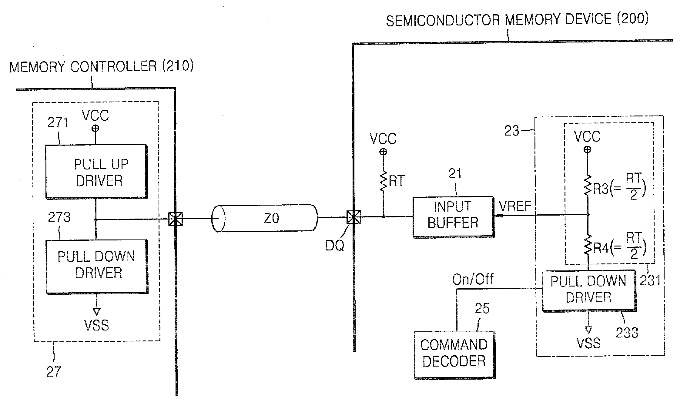
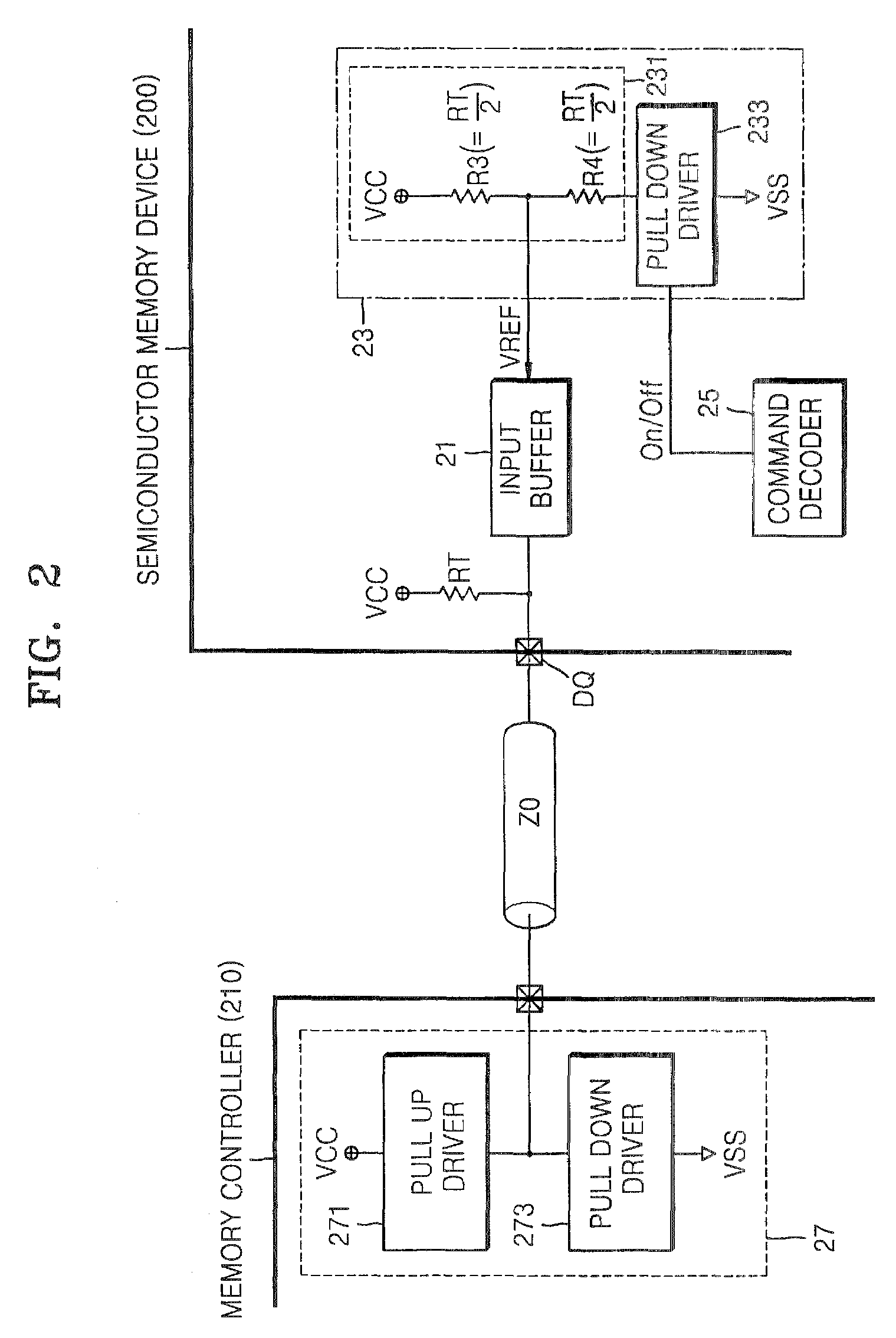
[0036]FIG. 2 is a block diagram of a semiconductor memory device 200 including an internal reference voltage generating circuit 23 according to an exemplary embodiment of the present invention. For the sake of descriptive convenience, a memory controller 210 that controls the semiconductor memory device 200 is illustrated.

[0037]Referring to FIG. 2, the semiconductor memory device 200 includes an input end DQ, an on die termination (ODT) resistor RT connected to the input end DQ, and an input buffer 21 that receives a signal input from the input end DQ based on a reference voltage VREF, wherein the internal reference voltage generating circuit 23 that generates the reference voltage VREF.

[0038]The input buffer 21 is a data input buffer that receives a...


PUM


Abstract

An internal reference voltage generating circuit that reduces a standby current and the number of pins of a semiconductor memory device, in which a reference voltage is provided to an input buffer that receives a signal through an input to which an on die transmitor resistor is connected, includes: a voltage dividing circuit outputting the reference voltage by a power voltage; a pull down driver connected to an end of the voltage dividing circuit; and a calibration control circuit comparing a voltage level of the input and a voltage level of an end of the voltage dividing circuit, and controlling the on resistor value of the pull down driver according to a result of the comparison. The internal reference voltage generating circuit is operated while the memory controller inputs a signal into a mode register set (MRS) to enable the internal reference voltage generating circuit and the output signal of the MRS is activated.

Description

CROSS-REFERENCE TO RELATED PATENT APPLICATION[0001]This application claims priority from Korean Patent Application No. 10-2005-0135870, filed on Dec. 30, 2005, in the Korean Intellectual Property Office, the disclosure of which is incorporated herein in its entirety by reference.BACKGROUND OF THE INVENTION[0002]1. Technical Field[0003]The present disclosure relates to a reference voltage generating circuit and, more particularly, to an internal reference voltage generating circuit for an input buffer of a high-speed semiconductor memory device, and a semiconductor memory device including the same.[0004]2. Discussion of the Related Art[0005]Owing to the development of mobile systems, the demand for semiconductor memory devices operated on a high-speed low voltage has increased. Conventional semiconductor memory devices operated on such a high-speed low voltage stably receive input signals having a small swing width using input buffers based on a predetermined reference voltage.[0006]...

Claims


Application Information

Patent Timeline
Patent Type & Authority Patents(United States)
IPC IPC(8): G11C5/14
CPCG11C5/147G05F3/02G11C7/1048
Inventor SEO, YOUNG-HUNSEO, DONG-ILLEE, KYU-CHANCHOI, JONG-HYUN
Owner SAMSUNG ELECTRONICS CO LTD
Why Eureka
Try Eureka