Substrate for an FBGA semiconductor component

a technology of semiconductor components and substrates, applied in semiconductor devices, semiconductor/solid-state device details, electrical apparatus, etc., can solve the problems of material cohesive connection fractures or tears of bonding wires, etc., to avoid housing fractures, increase the reliability of fbga semiconductor components, and low expenditure

Inactive Publication Date: 2009-04-14
POLARIS INNOVATIONS LTD
View PDF16 Cites 9 Cited by
  • Summary
  • Abstract
  • Description
  • Claims
  • Application Information

AI Technical Summary

Benefits of technology

[0011]Consequently, in one aspect, the invention avoids a housing fracture with a low expenditure in terms of time and costs and thus increases the reliability of FBGA semiconductor components.
[0012]According to embodiments of the invention, positively locking elements for a potting composition are arranged in that region in which the housing part is produced. By virtue of these positively locking elements, a positively locking joint is also effected in addition to the previously acting materially cohesive joint and thus on the one hand the stability of the housing part is increased and on the other hand the connection of the housing part to the substrate is improved. By virtue of this additional positively locking joint, a housing fracture and thus a fracture or a tearing-away of the wire bridges are effectively prevented, as a result of which the reliability of FBGA semiconductor components is increased.

Problems solved by technology

This materially cohesive connection has proved to be disadvantageous to the effect that fractures very often occur in this housing part.
These housing fractures lead to fractures or tears of the bonding wires in each case in the region of the housing fracture.
The consequence of this is that the semiconductor components have an excessively low reliability and thus do not meet the quality requirements.
The problem of housing fracture and low reliability has been combated hitherto by searching for suitable materials, which has led to the expensive development of new materials for minimizing stress.
This demand for the use of “universal” materials, that is to say those that can be utilized for entire technology platforms, exhibits a very high expenditure in terms of costs and time.

Method used


Image

  • Substrate for an FBGA semiconductor component
  • Substrate for an FBGA semiconductor component
  • Substrate for an FBGA semiconductor component

Examples


Embodiment Construction

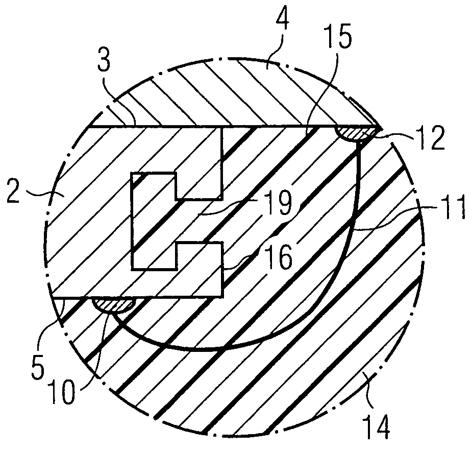
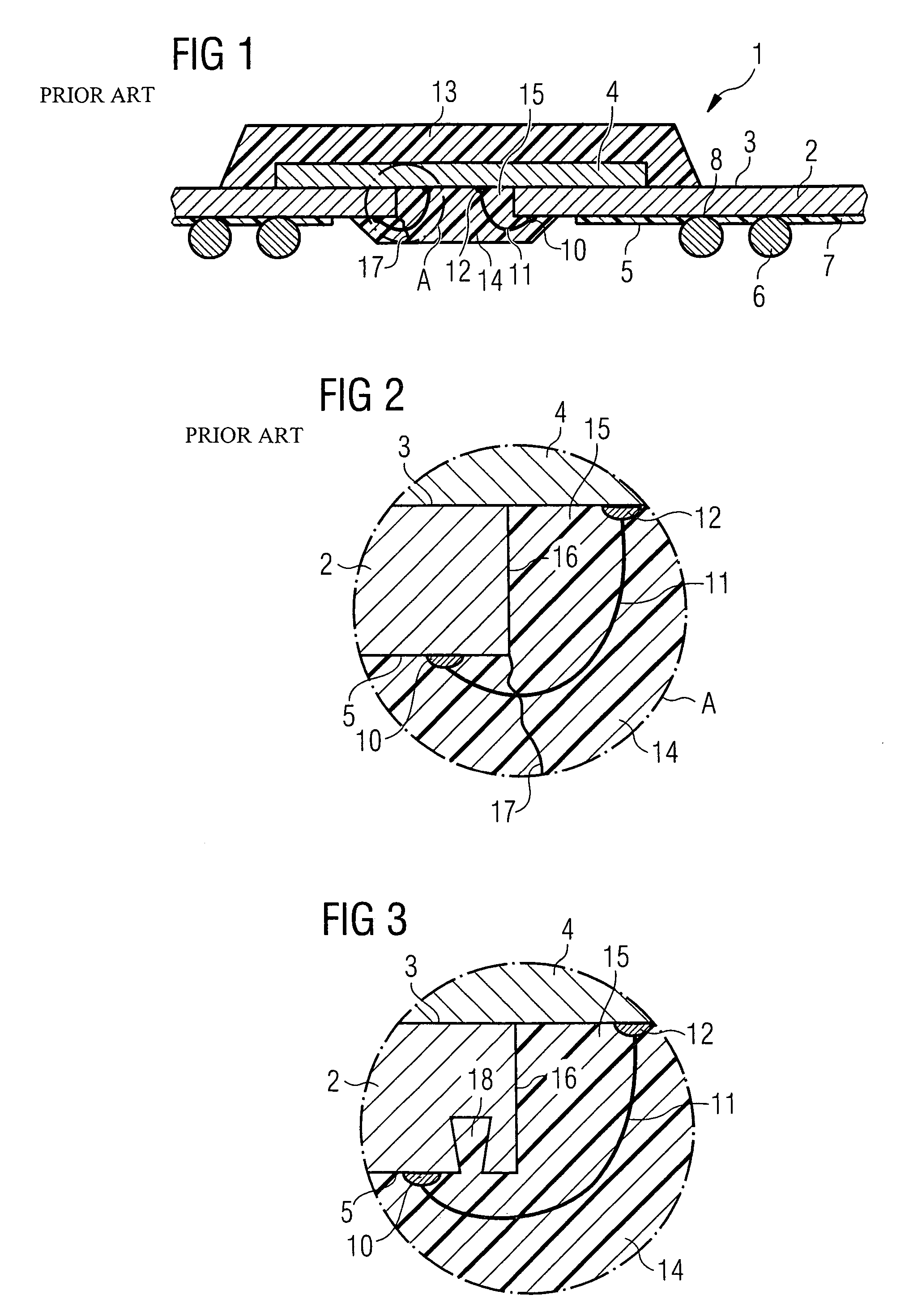
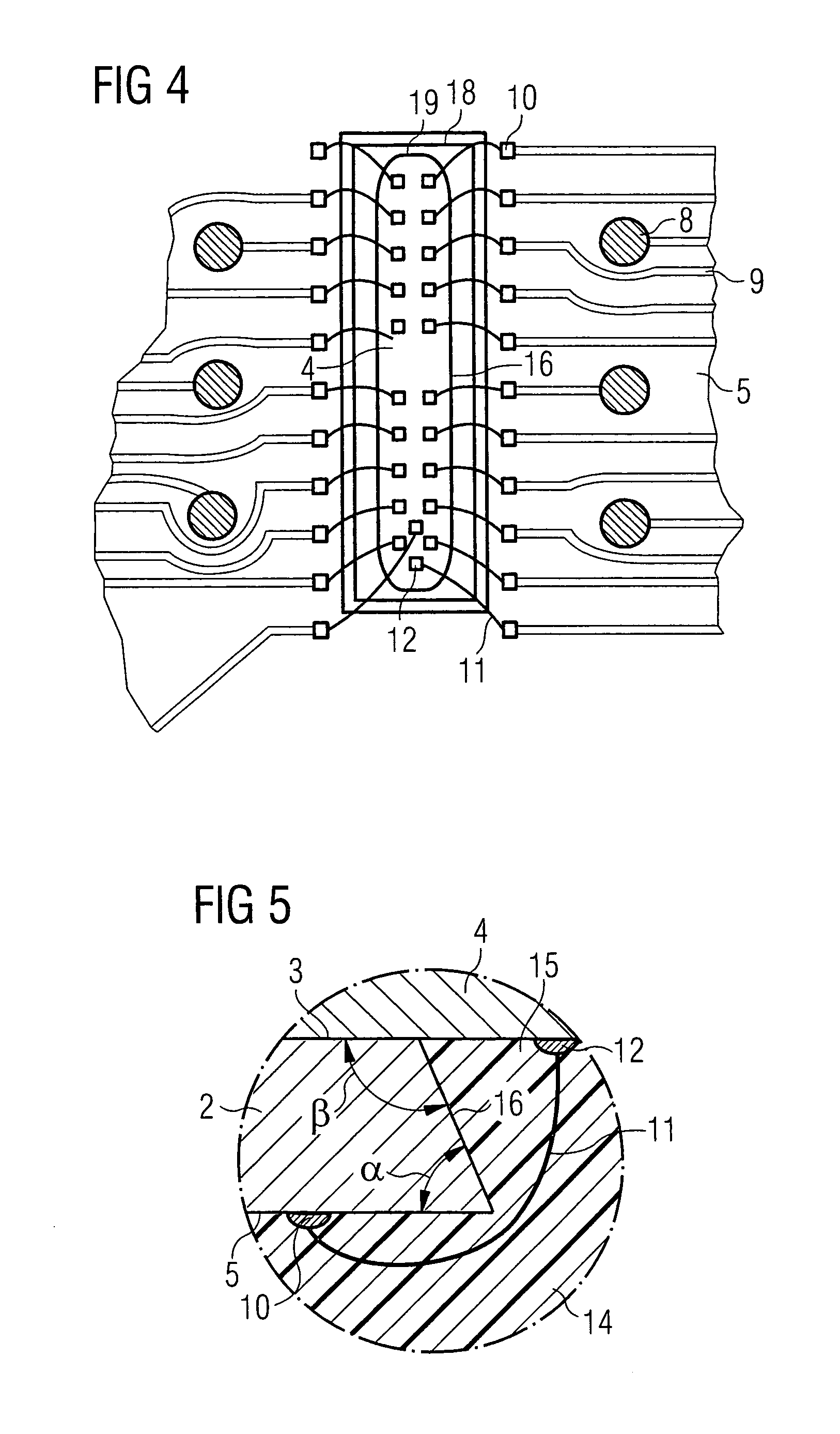
[0038]As illustrated in FIG. 1, an FBGA semiconductor component 1 contains a substrate 2. A semiconductor chip 4 is mounted on the chip side 3. The substrate 2 is provided with solder balls 6 on a solder ball side 5. In order to prevent solder from flowing away from the solder balls 6, a soldering resist mask 7 is furthermore applied to the solder ball side 5.

[0039]The solder balls 6 are fixed on ball pads 8. The ball pads 8 are electrically conductively connected to bonding pads 10 on the solder ball side 5 via a conductor structure 9 (shown in FIG. 4). For connecting the semiconductor chip 4 to the conductor structure 9, the bonding pads 10 are connected to bonding pads 12 on the semiconductor chip via wire bridges 11. For mechanical stabilization and for protection, the FBGA semiconductor component 1 is provided with a housing part 13, which covers the semiconductor chip 4, and with a housing part 14, which fills the bonding channel 15.

[0040]As illustrated in FIG. 1, the bonding ...


PUM


Abstract

An FBGA semiconductor component has a chip side for receiving a semiconductor chip, a solder ball side for applying solder balls on ball pads, and a bonding channel embodied as an opening between the chip side and the solder ball side and serving for leading through wire bridges between the semiconductor chip and bonding islands on the solder ball side. The bonding channel has side areas extending between the chip side and the solder ball side and can be closed off with a housing part comprising potting composition. Positively locking elements for a potting composition are arranged in that region of the substrate in which the housing part is produced.

Description

[0001]This application claims priority to German Patent Application 10 2005 003 390.3, which was filed Jan. 24, 2005, and is incorporated herein by reference.TECHNICAL FIELD[0002]The invention relates to a substrate for an FBGA semiconductor component.BACKGROUND[0003]Semiconductor chips are usually mounted to form semiconductor components for protection against external influences, for mechanical stabilization and for connection to an external circuit. So-called FBGA semiconductor components are known in this case. In this case, “FBGA” stands for “Fine Ball Grid Array,” which means that small solder balls are arranged in gridlike fashion in an array on a solder ball side of a substrate.[0004]The small solder balls are fixed on ball pads. The ball pads are part of a conductor structure that serves for the electrically conductive connection to bonding pads. The conductor structure with its ball pads and the bonding pads is usually likewise arranged on the solder ball side of the subst...

Claims


Application Information

Patent Timeline
Patent Type & Authority Patents(United States)
IPC IPC(8): H01L23/495
CPCH01L23/3128H01L23/3142H01L24/48H01L2224/05599H01L2224/48091H01L2224/4824H01L2224/48464H01L2224/48465H01L2224/49171H01L2224/85399H01L2924/01005H01L2924/01082H01L2924/014H01L2924/10156H01L2924/10157H01L2924/10158H01L2924/15311H01L2924/18301H01L2924/00014H01L24/49H01L2924/01033H01L2924/01068H01L2924/00H01L2224/45099H01L2224/05554H01L2924/181H01L2924/00012
Inventor KROEHNERT, STEFFENKAHLISCH, KNUTWAHRMUND, WIELAND
Owner POLARIS INNOVATIONS LTD
Why Eureka
Try Eureka