Waveguide structure for creating a phase gradient between input signals of a system of antenna elements

a waveguide and antenna element technology, applied in optical elements, particular array feeding systems, instruments, etc., can solve the problems of large space requirements for parallel plate guides and equalizing conductors, unsuitable industrial applications involving radar sensors, and relatively high losses in lenses, so as to achieve low-loss beam deflection and little space

Inactive Publication Date: 2009-04-14
ROBERT BOSCH GMBH
View PDF12 Cites 9 Cited by
  • Summary
  • Abstract
  • Description
  • Claims
  • Application Information

AI Technical Summary

Benefits of technology

[0007]The exemplary embodiment and / or exemplary method of the present invention provides a planar waveguide structure (concerning the type described above) that requires relatively little space and also allows relatively low-loss beam deflection.
[0012]According to an advantageous type of embodiment, on the signal plane and on the ground plane the conductive layers of the parallel plate guide end along a curved line that forms the reflector contour. However, the curved-shaped reflector contour of the parallel plate guide may also be realized as appropriately arranged conductive through-channels between the conductive layers on the signal side and on the ground side, it being necessary for the distance between these through-channels, and the diameter of the through-channels, to be small relative to the wavelength of the guided wave. It is particularly advantageous if the curvature of the reflector contour is approximately parabolic. It is important to note that the focusing properties of the waveguide structure according to the exemplary embodiment and / or exemplary method of the present invention may be improved even further if the design deviates from a parabolic shape. Numerical optimization methods may be used to determine a reflector contour that evenly minimizes phase deviations at the focal points.
[0013]According to a particularly advantageous embodiment of the waveguide structure according to the exemplary embodiment and / or exemplary method of the present invention, microstrip conductors are provided in the conductive layer, which are connected to the beam lobe ports of the parallel plate guide via planar feed horns (guide tapers). It was found that bundling and irradiation can be determined based on the size of the feed horns, which helps reduce loss. Moreover, irradiation occurs only to a limited extent, thanks to the shape of the reflector structure.
[0016]According to an advantageous further refinement of the waveguide structure according to the exemplary embodiment and / or exemplary method of the present invention, dummy ports are provided in the conductive layer within the contour of the parallel plate guide. Dummy ports in the area between the beam lobe ports are used to decouple individual beam lobe ports from one another. Providing dummy ports in the area between the beam lobe ports and the reflector contour prevents undesirable reflection. These dummy ports too are advantageously in the form of planar feed horns, which are each closed off to ensure low reflection or lead to a low-reflection closed-off conductor.

Problems solved by technology

The lens structure just described has various disadvantages which may make it unsuitable for industrial applications involving radar sensors.
Losses in the lenses, in particular due to the equalizing conductors, are relatively high.
Furthermore, parallel plate guides and equalizing conductors require a relatively large amount of space.
As a general rule, there is a relatively large amount of irradiation loss at the sides of the lens structure and from the parallel plate guide.
This means the sensor has to be relatively long in the direction of elevation, which is not favorable for automotive applications.

Method used


Image

  • Waveguide structure for creating a phase gradient between input signals of a system of antenna elements
  • Waveguide structure for creating a phase gradient between input signals of a system of antenna elements
  • Waveguide structure for creating a phase gradient between input signals of a system of antenna elements

Examples


Embodiment Construction

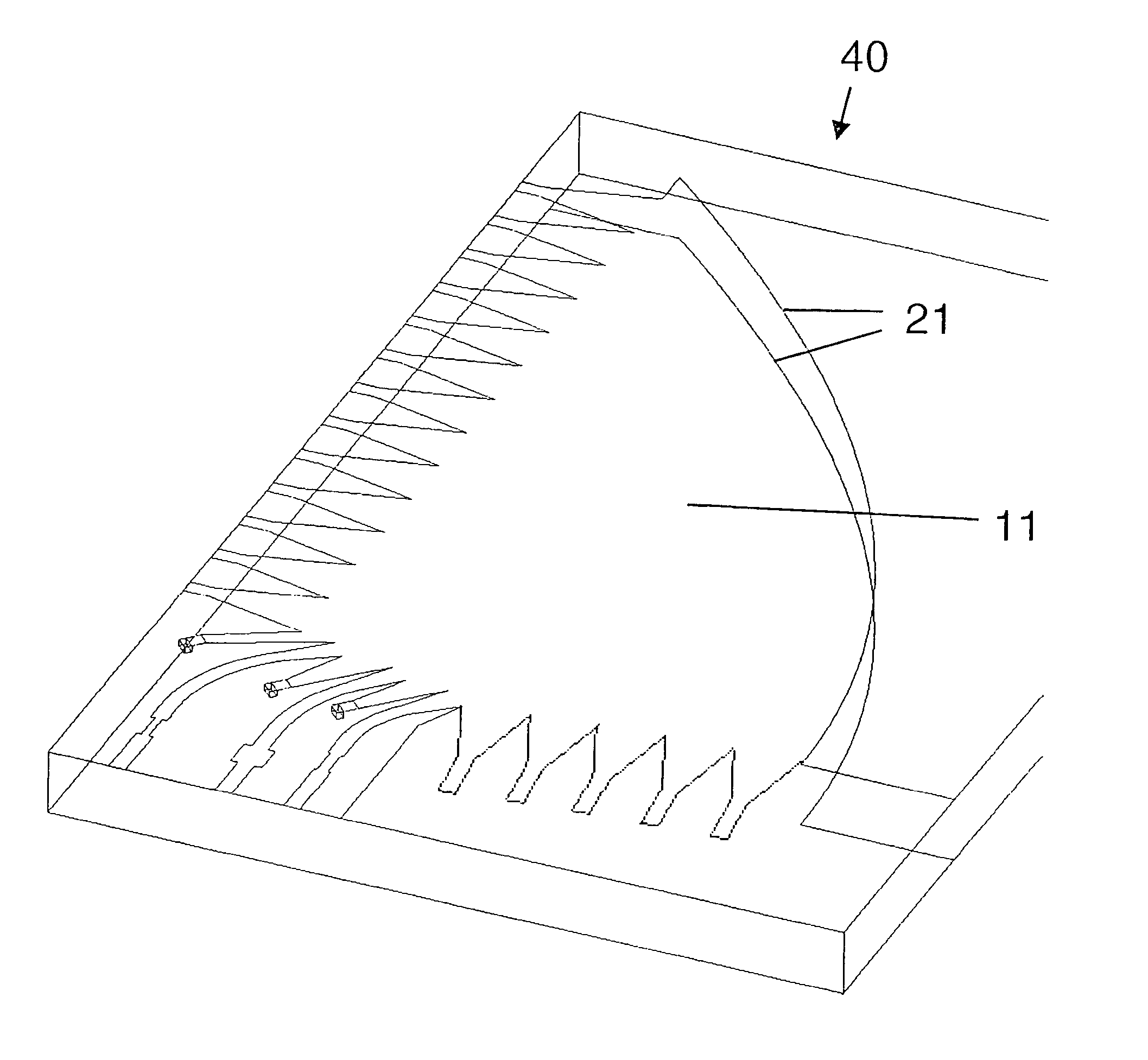
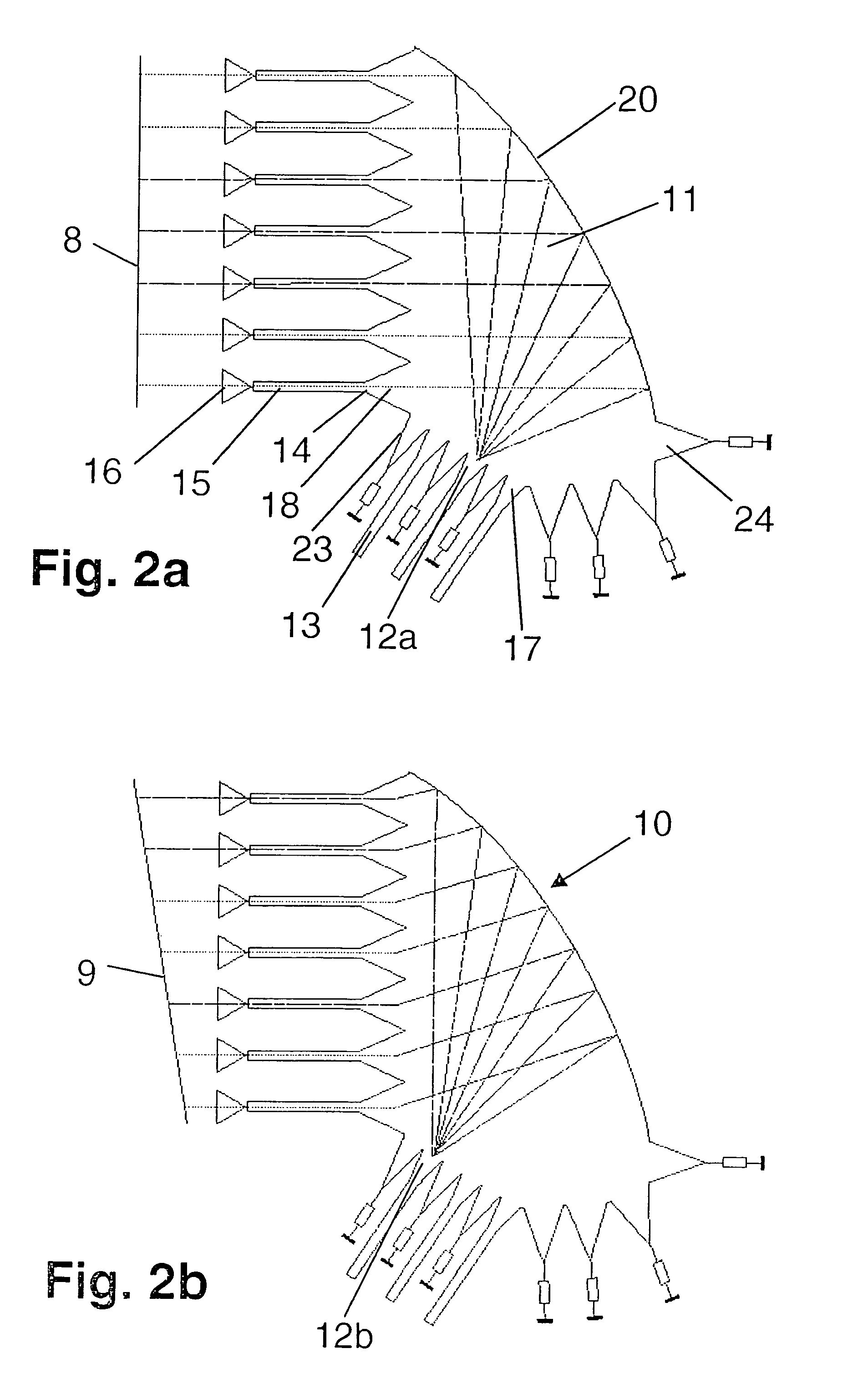
[0024]The waveguide structure 10 shown in FIGS. 2a and 2b is used to create a phase gradient between the input signals of a system of antenna elements 16.

[0025]Waveguide structure 10 is implemented using microstrip technology, as used in the manufacture of inexpensive high-frequency circuits. In the simplest case, a single-layer microwave substrate made of ceramic material, glass or filled plastic and metal plated on both sides is used. Parallel plate guide 11 having beam lobe ports 12 for signal feed and signal pickup is created by structuring the upper surface, which constitutes the signal side of waveguide structure 10 and is shown here. The metal plated bottom side serves as the ground of waveguide structure 10 and may also be structured. According to the exemplary embodiment and / or exemplary method of the present invention, parallel plate guide 11 has a curved-shaped reflector contour 20 so that it functions as a signal reflector. The curvature of reflector contour 20 is approx...


PUM


Abstract

A planar waveguide structure for creating a phase gradient between the input signals of a system of antenna elements requires relatively little space and also ensures relatively low-loss beam deflection. The waveguide structure is provided on a dielectric microwave substrate, which has at least one conductive layer on both sides. At least one of the two conductive layers is structured and constitutes the signal side of the wave structure, while the other conductive layer is used as ground. The waveguide structure includes at least one parallel plate guide having beam lobe ports for signal feed and signal pickup. This parallel plate guide has a curved-shaped reflector contour so that it functions as a signal reflector.

Description

FIELD OF THE INVENTION[0001]The present invention relates to a waveguide structure for creating a phase gradient between the input signals of a system of antenna elements. The waveguide structure is provided on a dielectric microwave substrate which has at least one conductive layer on both sides. At least one of the two conductive layers is structured and constitutes the signal side of the waveguide structure, while the other conductive layer is used as ground. The waveguide structure includes at least one parallel plate guide having beam lobe ports for signal feed and signal pickup.BACKGROUND INFORMATION[0002]In industrial applications, waveguide structures of this kind are used to create phased arrays in the microwave range. Due to the phase gradient φ between the input signals of adjacent antenna elements, their output signals are subject to phase lead / lag, and in consequence the azimuthal angle of the resulting phase front of the antenna output signal wave is modified.[0003]The...

Claims


Application Information

Patent Timeline
Patent Type & Authority Patents(United States)
IPC IPC(8): H01Q13/00H01Q15/02H01Q15/24H01Q19/06H01Q1/32H01Q1/38H01Q21/00H01Q25/00
CPCH01Q1/3233H01Q1/38H01Q21/0031H01Q25/008
Inventor SCHOEBEL, JOERG
Owner ROBERT BOSCH GMBH
Why Eureka
Try Eureka