Methods for slow test time detection of an integrated circuit during parallel testing

a technology of integrated circuit and parallel testing, applied in the direction of electrical testing, measurement devices, instruments, etc., can solve the problems of test failure, aberrant circuit behavior, and greatly degraded performance of any given devi

Active Publication Date: 2009-05-05
OPTIMAL PLUS
View PDF32 Cites 8 Cited by
  • Summary
  • Abstract
  • Description
  • Claims
  • Application Information

AI Technical Summary

Problems solved by technology

Such variation is generally unavoidable in IC fabrication processes, and results in a distribution of electrical performance in a population of finished IC devices that is usually “normal”, i.e. Gaussian, in nature.
Moreover, the performance of any given device can also be greatly degraded by faulty fabrication processing, potentially creating or depositing discrete defects within the circuits of the device or skewing the dimensions of IC sub-component structures, leading to aberrant circuit behavior.
In most cases, such issues will actually cause the finished IC device to be non-functional, resulting in test failure.
However, if the issue is relatively minor the device may remain functional, and will simply exhibit highly degraded electrical performance.
The problem of slow device test time is exacerbated by the trend in IC test technology towards higher levels of test parallelism.
As the number of devices included in a parallel group increases, with advancing IC manufacturing and test technology, so does the probability that at least one of those devices will exhibit abnormally slow test-time.
For example, if 1% of individual devices contain fabrication defects causing them to be abnormally slow to test, the probability of finding such a device in a parallel test group sized at 16 devices is fairly low, while the probability of finding such a device in a parallel test group sized at 256 devices is highly likely.
As illustrated above, even when the fraction of abnormally slow-to-test devices is relatively low, the aberrant devices may have a significant impact on the overall test time of the test operation, especially in a highly parallel test environment.
Further, those skilled in the art will recognize that there is frequently a correlation between devices with abnormal behavior during test and the likelihood of ultimately either failing test operations or exhibiting reliability or performance problems in end-user product applications.
Therefore, test capacity in an IC test operation may be significantly limited by abnormal devices, which may individually have little or no value, or in a worse case may in fact contribute to product line reliability or performance issues.

Method used


Image

  • Methods for slow test time detection of an integrated circuit during parallel testing
  • Methods for slow test time detection of an integrated circuit during parallel testing
  • Methods for slow test time detection of an integrated circuit during parallel testing

Examples


Embodiment Construction

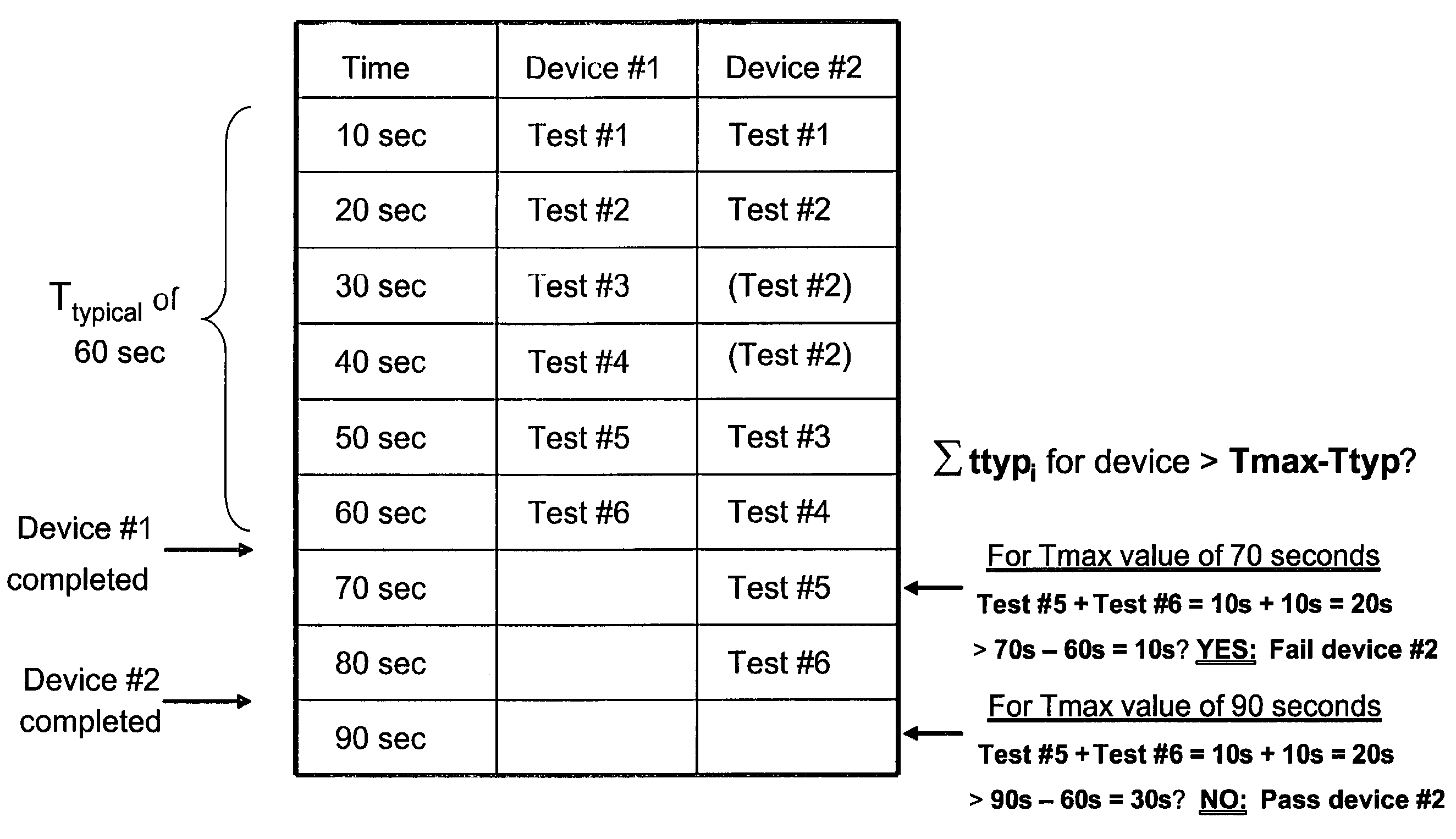
[0046]Described herein are embodiments of the current invention for semiconductor testing, including methods and systems that will automatically and in “real-time” identify devices exhibiting abnormally long test time (also termed below as too-slow testing devices, devices testing too slowly, abnormal devices or aberrant devices) during the course of testing. The forced early termination of the testing of such devices is facilitated under circumstances which depend on the embodiment, allowing test operations to progress sooner to the next untested device or group of devices to improve a test operation's overall efficiency.

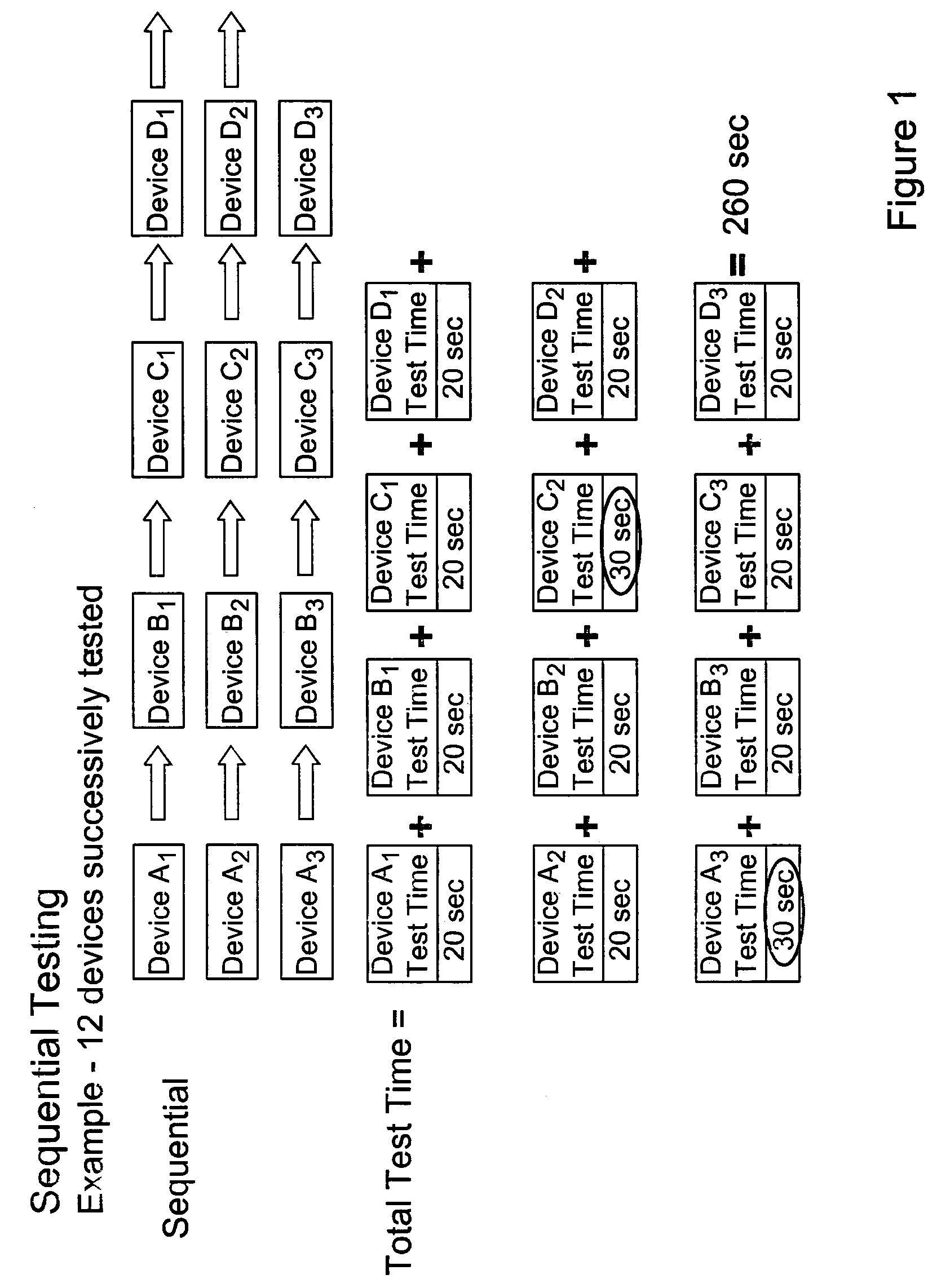
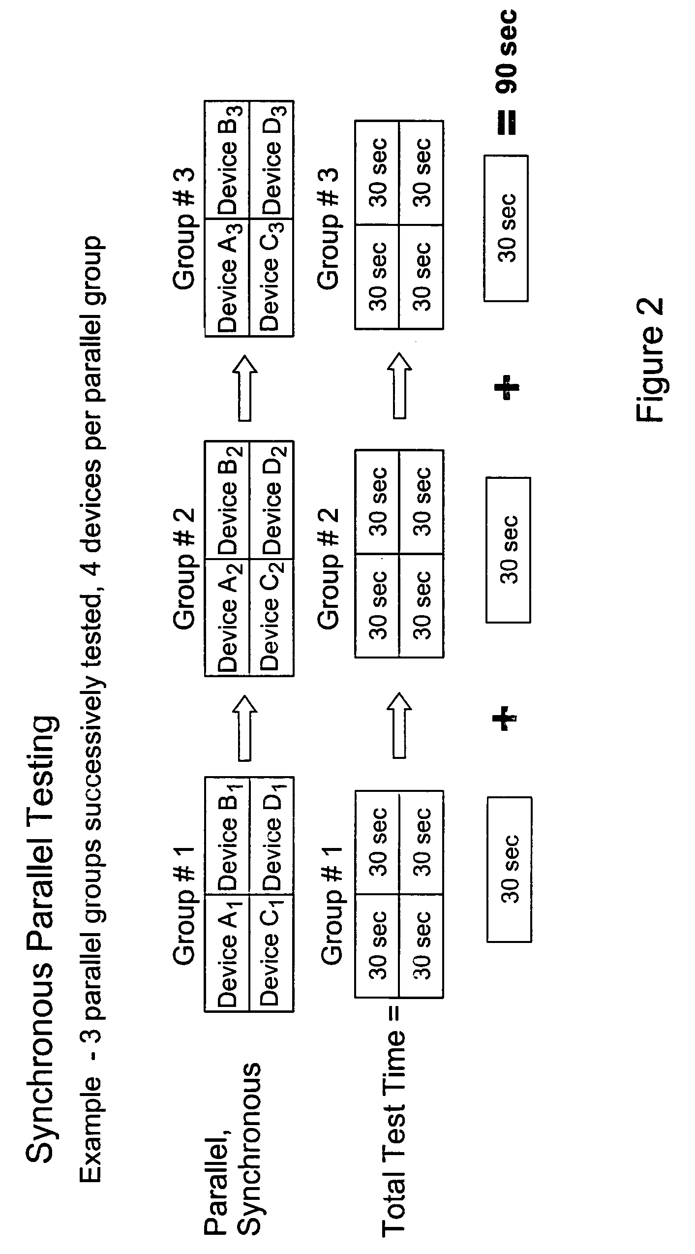
[0047]Test capacity is defined as the volume of material (i.e. number of devices) that can be processed through a factory test operation within a fixed period of time given the available test equipment and test times for that operation. Assuming that the available test equipment remains unchanged, increased test capacity (for example through the lowering of test ti...


PUM


Abstract

Methods and systems for semiconductor testing are disclosed. In one embodiment, devices which are testing too slowly are prevented from completing testing, thereby allowing untested devices to begin testing sooner.

Description

CROSS REFERENCE TO RELATED APPLICATIONS[0001]This application is a continuation in part of co-pending U.S. application Ser. No. 11 / 175,026 filed on Jul. 6, 2005, which is hereby incorporated by reference herein.FIELD OF THE INVENTION[0002]This invention relates to semiconductor integrated circuit testing.BACKGROUND OF THE INVENTION[0003]Some terms used in semiconductor testing industry will now be illuminated. The definitions are presented informally to aid in the understanding of the reader and therefore should not be considered binding:[0004]An integrated circuit (IC) is a small electronic device made out of a semiconductor material.[0005]A wafer is a thin slice of semiconductor material, such as silicon, upon which microcircuits are constructed by doping (for example, diffusion or ion implantation), etching, and deposition of various materials.[0006]A wafer is usually made up of many single units also called dice (one unit=die, two or more units=dice or dies). After the fabricati...

Claims


Application Information

Patent Timeline
Patent Type & Authority Patents(United States)
IPC IPC(8): G01R31/26
CPCG01R31/3172G01R31/31707G01R31/318511G01R31/2601G01R31/2894
Inventor BALOG, GILLINDE, REEDGOLAN, AVI
Owner OPTIMAL PLUS
Why Eureka
Try Eureka