Micro-optic elements and method for making the same

a technology of micro-optic elements and micro-lens arrays, applied in the field of micro-optic elements, can solve the problems of unwanted light dispersions, the known methods of producing micro-lenses and micro-lense arrays cannot effectively produce lenses with a specific profile, etc., and achieve the effect of convenient configuration

Inactive Publication Date: 2009-05-12
HWU RUEY JEN
View PDF30 Cites 18 Cited by
  • Summary
  • Abstract
  • Description
  • Claims
  • Application Information

AI Technical Summary

Benefits of technology

[0006]Next, the substrate and photo-resist are exposed to a stripping process to remove the remaining photo-resist from the substrate. When the photo-resist is completely stripped from the substrate, the resultant structure is in the form of a micro-lens or a micro-lens array disposed on the surface of the substrate. As a

Problems solved by technology

Unfortunately, prior art methods produce many optical elements having deviations that cause unwanted light dispersions.
In addition, known methods of

Method used


Image

  • Micro-optic elements and method for making the same
  • Micro-optic elements and method for making the same
  • Micro-optic elements and method for making the same

Examples


Embodiment Construction

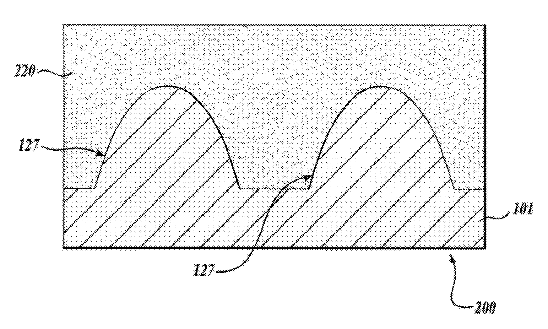
[0016]The present invention relates to micro-optic elements and a method for making the same. In one aspect of the present invention, the method for making micro-optic elements involves a reactive ion etching process having controlled process parameters, such as a predetermined photo-resist depth and etch-rate selectivity. As a result of a predetermined photo-resist depth and selectivity, one embodiment of the fabrication process forms a micro-optic element having a predetermined shape, such as an elliptical or a parabolic shape. In another embodiment of the present invention, a micro-lens having a curved cross-section is used to construct micro-mirrors—also referred to as external cavities. The resultant profile of the external cavity formed in this embodiment reduces the filamentation of a laser and promotes the single mode operation of a high-power, broad area semiconductor laser.

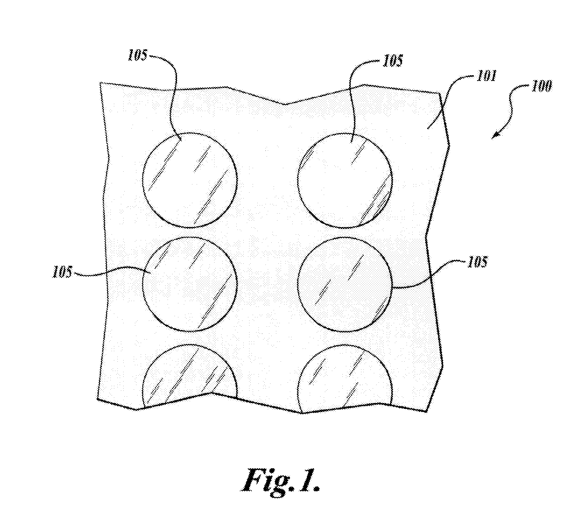
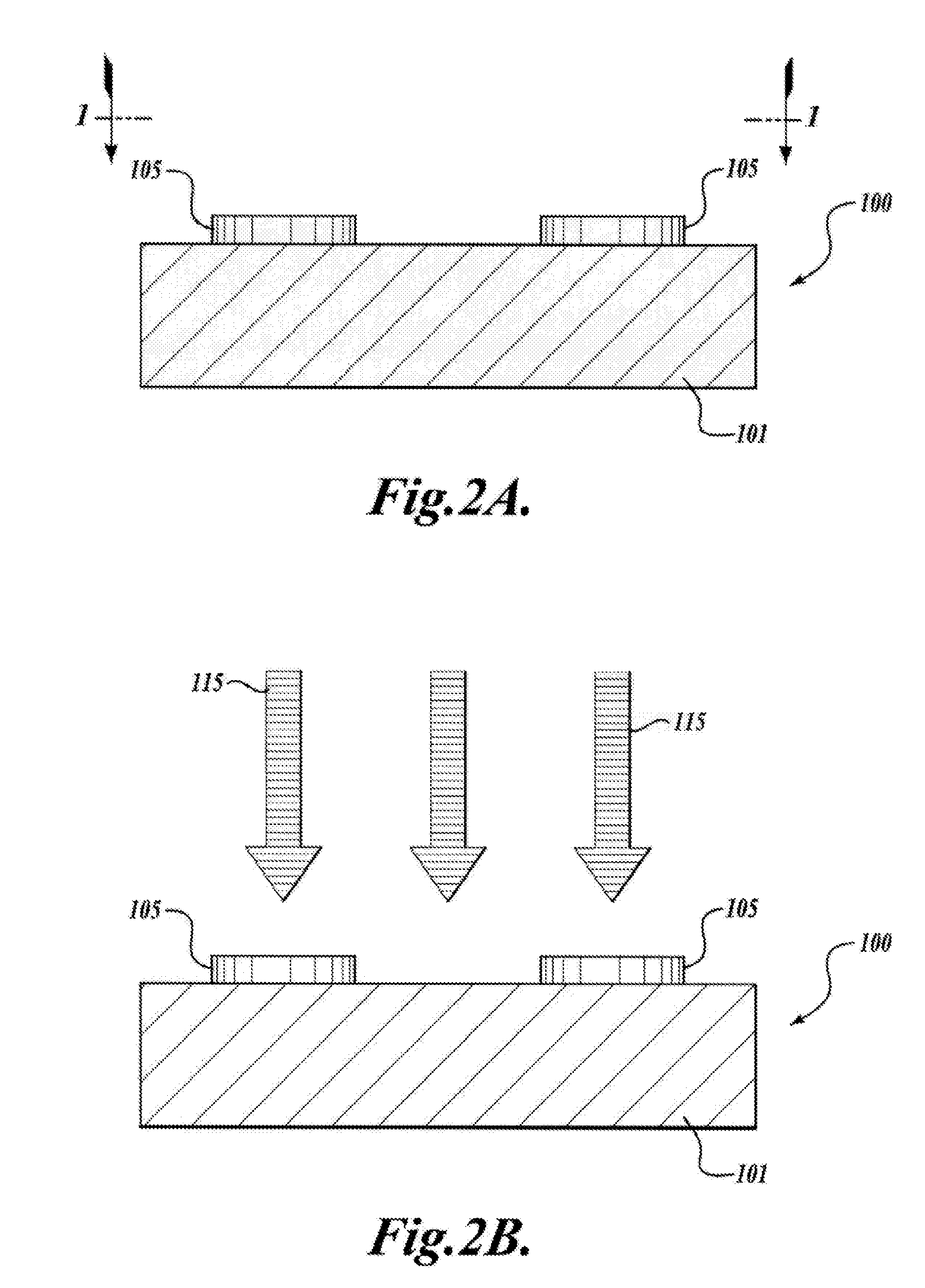
[0017]Referring now to FIGS. 1 and 2A, one embodiment of a fabrication process for forming a micro-op...


PUM

PropertyMeasurementUnit
Diameteraaaaaaaaaa
Diameteraaaaaaaaaa
Magnetic fieldaaaaaaaaaa

Abstract

A method of making micro-optic elements. In one embodiment, photo-resist elements each having predetermined dimensions are transferred onto a substrate. The photo-resist elements are exposed to a reflow process to shape the top surface of the elements into a curved surface. The method also involves a reactive ion etching process having controlled parameters, such as a photo-resist depth and the selectivity between the substrate and photo-resist. A predetermined photo-resist depth and selectivity form a micro-optic element having a predetermined shape, preferably an elliptical or parabolic shape. In another aspect of the present invention, a micro-optic element is used to construct a micro-mirror for eliminating filamentation and promoting single mode operation of high-power broad area semiconductor lasers. The lenses and micro-mirrors produced by methods disclosed herein are configured to collimate the output of high-power lasers and promote a Gaussian intensity profile laser beam from a broad area laser beam.

Description

FIELD OF THE INVENTION[0001]The present invention is related to micro-optic elements (MOE) and, more particularly, to elliptical and parabolic micro-optic elements, such as micro-lenses, micro-lens arrays (MLA), micro-reflectors, and micro-mirrors made by reactive ion etching (RIE).BACKGROUND OF THE INVENTION[0002]In recent years, interest in the field of micro-optics has continued to increase. For instance, miniature lenses, micro-lenses, and micro-lens arrays are in demand for applications involving optical computing, optical information processing, and communications. In one specific example, micro-lenses and micro-lens arrays are used in various apparatuses for coupling light from a laser to an optical fiber and coupling light from an optical fiber to a photo-detector. In another example, a micro-reflector or a micro-mirror may be used to direct the light or construct external cavities. Several embodiments of an apparatus where a parabolic reflector is used to promote single tra...

Claims


Application Information

Patent Timeline
IPC IPC(8): C23F1/00G02B3/00G03F7/00G03F7/40
CPCG02B3/0018G02B3/0056G03F7/0005G03F7/40
Inventor HWU, RUEY-JEN
Owner HWU RUEY JEN
Why Eureka
Try Eureka