Method and system for integrated DWDM receivers

a receiver and optical technology, applied in the field of fiber optical transport systems, can solve problems such as restricting the effectiveness of broader applications, and achieve the effect of reducing the size and cost of optical transport systems and broader range of applicability

Active Publication Date: 2009-05-12
FUTUREWEI TECH INC
View PDF4 Cites 5 Cited by
  • Summary
  • Abstract
  • Description
  • Claims
  • Application Information

AI Technical Summary

Benefits of technology

[0008]The present invention is directed to fiber optical transport systems. More particularly, the invention provides a method and system for an integrated optical receiver for reducing the size and cost of optical transport systems. Merely by way of example, the invention has been applied to DWDM optical transport systems employing InP photodetectors. But it would be recognized that the invention has a much broader range of applicability.
[0017]Many benefits are achieved by way of the present invention over conventional techniques, such as a monolithically integrated DWDM receiver on an InP substrate. For example, in certain embodiments, an embodiment of the invention provides a method and system for integrating semiconductor InP photodetector chips with a silica / silicon AWG substrate for reducing the size and cost of the terminals of optical transport systems. Because the processing cost per unit area for silica-on-silicon can be two orders of magnitude lower than that for InP, the AWG according to embodiments of the present invention can be made at much lower cost. Silica-on-silicon AWGs is a much more mature technology. For example, transmission loss is much smaller in AWGs made of silica-on-silicon than those made of InP. Because there are much fewer elements on the InP chip according to embodiments of the invention, compared to the conventional InP monolithic integration method, the InP chip fabrication yield is much higher. Without AWG, the InP chip is also much smaller, according to an embodiment of the invention. The high yield and the small size significantly reduce the cost of the InP chips used for hybrid integration in accordance to embodiments of the present invention.
[0018]According to certain embodiments of the present invention, a method is provided for using surface illuminated APDs which can results in >=10 dB increase in receiving sensitivity than conventional techniques. This improvement can enable long distance transmission without optical amplifiers. Further, in term of finished device, the size of a hybrid integrated DWDM receiver according to specific embodiments of the invention is comparable to that of a monolithically integrated DWDM receiver. Thus the small size advantage of an integrated DWDM receiver is retained according to certain embodiments of the present invention.

Problems solved by technology

Even though these conventional DWDM systems are useful in some areas, they have many limitations that restrict their effectiveness in broader applications.

Method used


Image

  • Method and system for integrated DWDM receivers
  • Method and system for integrated DWDM receivers
  • Method and system for integrated DWDM receivers

Examples


Embodiment Construction

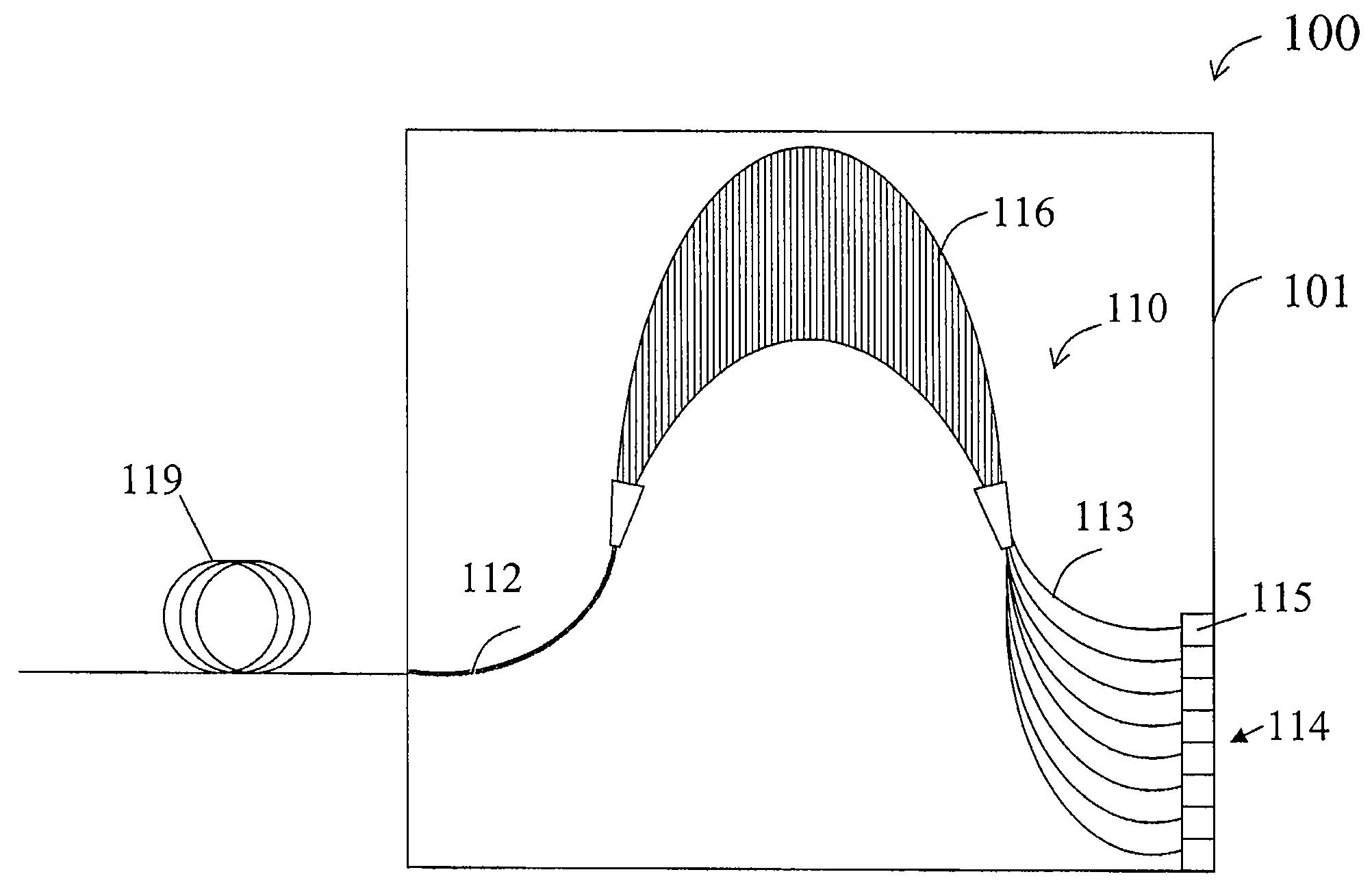
[0027]The present invention is directed to fiber optical transport systems. More particularly, the invention provides a method and system for an integrated optical receiver for reducing the size and cost of optical transport systems. Merely by way of example, the invention has been applied to DWDM optical transport systems employing InP photodetectors. But it would be recognized that the invention has a much broader range of applicability.

[0028]The optical components in a conventional DWDM system are usually individually packaged. To a great extent, the packaging cost determines the price of the components. For example, the cost of a high speed (>˜10 Gbps) bare PIN chip cost only a few dollars, while a packaged PIN sells for several hundred dollars, mostly due to the cost of packaging. It is thus difficult to further reduce the cost with the conventional DWDM system design. In addition, the multiple linecards, each built with the individual components, make it difficult to reduce th...


PUM


Abstract

An integrated DWDM receiver apparatus includes a support component and a silica-on-silicon substrate overlying the support component. The substrate includes a silica layer overlying a silicon layer and includes a first surface region and a second surface region. An optical demultiplexer is disposed within the silica layer under the first surface region and overlying the silicon layer. The optical demultiplexer includes a plurality of output waveguides and at least an input waveguide. The receiver apparatus includes one or more reflecting structures located in the silica layer under the second surface region. Each of the reflecting structures is optically coupled to a corresponding output waveguide. The receiver apparatus also includes one or more semiconductor photodetector array chips overlying the second surface region of the silica-on-silicon substrate. Each of the one or more photodetector array chips including one or more photodetectors which is optically coupled to a corresponding reflecting structure.

Description

CROSS-REFERENCES TO RELATED APPLICATIONS[0001]This application claims priority to U.S. Provisional Patent Application No. 60 / 829,009, filed Oct. 11, 2006, commonly assigned, incorporated by reference herein for all purposes.[0002]Additionally, this application is related to U.S. patent application Ser. No. 11 / 696,472, filed Apr. 4, 2007, commonly assigned, incorporated by reference herein for all purposes.STATEMENT AS TO RIGHTS TO INVENTIONS MADE UNDER FEDERALLY SPONSORED RESEARCH OR DEVELOPMENT[0003]Not ApplicableREFERENCE TO A “SEQUENCE LISTING,” A TABLE, OR A COMPUTER PROGRAM LISTING APPENDIX SUBMITTED ON A COMPACT DISK[0004]Not ApplicableBACKGROUND OF THE INVENTION[0005]The present invention is directed to fiber optical transport systems. More particularly, the invention provides a method and system for an integrated optical receiver for reducing the size and cost of optical transport systems. Merely by way of example, the invention has been applied to dense wavelength division ...

Claims


Application Information

Patent Timeline
Patent Type & Authority Patents(United States)
IPC IPC(8): G02B6/12H04B10/43
CPCG02B6/12019G02B6/12026H04B10/25H04B10/67G02B6/4214
Inventor BAI, YU SHENG
Owner FUTUREWEI TECH INC
Why Eureka
Try Eureka