Production method for electroluminescent element

a production method and technology of electroluminescent elements, applied in the manufacture of electrode systems, electric discharge tubes/lamps, instruments, etc., can solve the problems of difficult to exert the function of photoresist peeling solution on the photoresist layer, and the inability to provide a manufacturing method for el elements, so as to prevent the damage of the substrate or the like by the solution

Inactive Publication Date: 2009-05-19
DAI NIPPON PRINTING CO LTD
View PDF14 Cites 18 Cited by
  • Summary
  • Abstract
  • Description
  • Claims
  • Application Information

AI Technical Summary

Benefits of technology

[0022]In the present invention, since the peeling layer having the excellent peeling property is provided on the organic EL layer, the peeling layer can be peeled off easily in the peeling layer peeling process. And thus, the other layers disposed on the peeling layer can be removed with the peeling layer easily at the same time. Therefore, the unnecessary layers such as the photoresist layer, which have hardly been peeled off conventionally, can be peeled off easily.
[0025]In the above mentioned invention, it is preferable that the peeling layer is soluble to the photoresist developing agent used for developing the photoresist layer, and the organic EL layer is insoluble to the photoresist developing agent. At the time of patterning the photoresist layer, the peeling layer can also be developed by the photoresist developing agent at the same time with the photoresist layer. And a trouble of swelling and eluting of the organic EL layer by the photoresist developing agent at the time can be avoided.
[0026]In the above mentioned invention, it is preferable that a film thickness of the peeling layer is in a range of 0.05 μm to 5 μm. Since the peeling layer, which is peeled off by bringing into contact with the peeling layer peeling solution has the film thickness within the above mentioned range, the contacting area with the peeling layer peeling solution can be ensured sufficiently so that the peeling layer can be peeled off quickly.
[0028]Moreover, in the above mentioned invention, it is preferable that the organic EL layer developing process is a process of using a dry etching method. By using the dry etching method, since the substrate or the like needs not to be soaked in the solution or the like in the organic EL layer forming process, damage of the substrate or the like by the solution can be prevented.

Problems solved by technology

However, by these methods, it has been impossible to provide a method for manufacturing an EL element, capable of realizing all of a high light emitting efficiency, a high light taking out efficiency, manufacturing process simplicity, and a high-definition pattern formation.
However, even in the case of the photolithography method having the advantages, at the time of completing patterning of the light emitting layer and peeling off the photoresist layer, a problem may be involved in that the peeling operation cannot be carried out easily.
This derives from a difficulty in selecting the photoresist peeling solution for peeling off the photoresist layer, because the solvent is limited to that satisfies the condition where in the organic EL layer is not soluble and the photoresist layer is soluble.
Also, when the contacting area of the photoresist peeling solution and the photoresist layer is small, it is difficult to exert the function of the photoresist peeling solution to the photoresist layer.
However, even when the method is employed, it is difficult to peel the photoresist layer off preferably.
Moreover, in contrast, a new problem of damaging the substrate or the like is generated.

Method used


Image

  • Production method for electroluminescent element
  • Production method for electroluminescent element
  • Production method for electroluminescent element

Examples


first embodiment

(1) First Embodiment

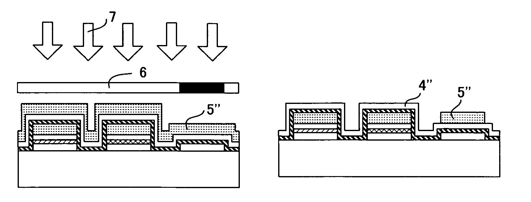
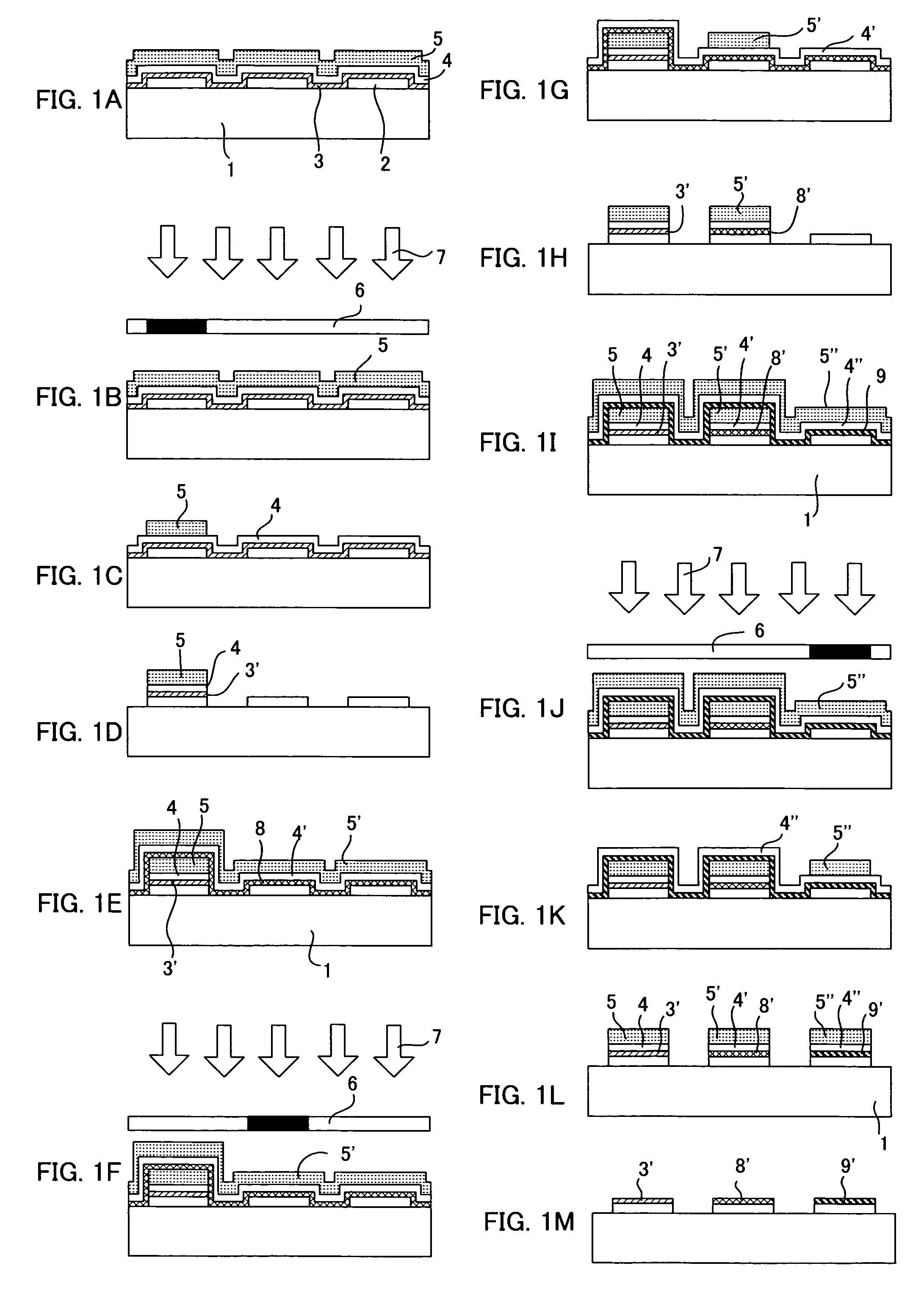
[0121]The first embodiment is an embodiment of patterning each light emitting part such that a light emitting part having a color different from the light emitting part is not laminated on each light emitting part when the patterning of each light emitting part is completed.

[0122]FIGS. 1A to 1M show an example of the method for manufacturing an EL element of the first embodiment. Hereinafter, FIGS. 1A to 1M will be explained specifically.

[0123]First, as shown in FIG. 1A, a first light emitting layer forming coating solution is coated on a substrate 1 having an electrode 2 formed in a pattern, so as to form a first light emitting layer 3 (first light emitting layer forming process). A peeling layer forming coating solution is coated on the first light emitting layer 3 so as to form a first peeling layer 4 (first peeling layer forming process). And furthermore, a positive type photoresist is coated on the first peeling layer 4 so as to form a first photoresist laye...

second embodiment

(1) Second Embodiment

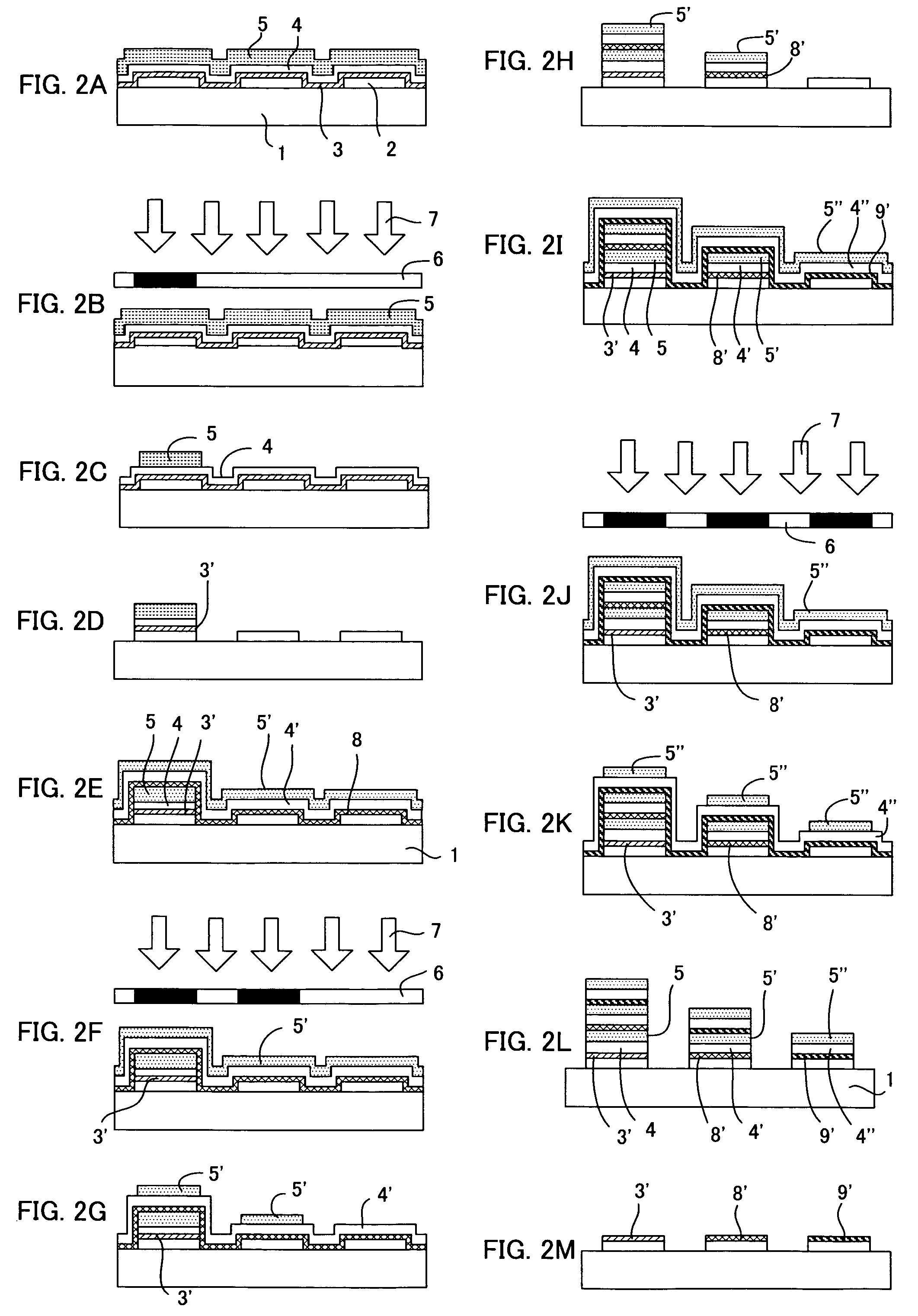
[0144]The second embodiment is an embodiment of exposing an ultraviolet ray via a mask, in the pattern irradiation carried out when patterning each three color of light emitting layers, such that a photoresist layer disposed on an area where the light emitting part, which is a subject to be patterned, will be formed and on the light emitting part already formed in a pattern remains.

[0145]That is, when patterning the second light emitting layer, the pattern irradiation is carried out such that the photoresist layer remains on the area, where the second light emitting part will be formed, and on the first light emitting part already formed in a pattern.

[0146]FIGS. 2A to 2M show an example of the method for manufacturing an EL element of such second embodiment. Hereinafter, FIGS. 2A to 2M will be explained specifically.

[0147]First, as shown in FIG. 2A, a first light emitting layer forming coating solution is coated on a substrate 1, having an electrode 2 formed in ...

example 1

[0167]A patterned ITO substrate of a 6 inch square and 1.1 mm plate thickness was cleaned. 0.5 ml of a buffer layer coating solution (Baytron P manufactured by Bayer Yakuhin, Ltd.) was taken and dropped onto the central part of the substrate and carried out a spin coating. By maintaining at 2,500 rpm for 20 seconds, a layer was formed. As a result, the film thickness was 800 Å.

[0168]As the first light emitting layer, 1 ml of a 1 wt % xylene solution of a polyparaphenylene vinylene derivative light emitting polymer MEH-PPV was taken on the buffer layer, and dropped onto the central part of the substrate and carried out the spin coating. By maintaining at 2,000 rpm for 10 seconds, a layer was formed. As a result, the film thickness was 800 Å.

[0169]As the peeling layer, 1 ml of a 3% ethyl acetate solution of a urea based resin (Laropal manufactured by BASF) was taken and dropped onto the central part of the substrate and carried out the spin coating. By maintaining at 2,000 rpm for 20 ...


PUM

PropertyMeasurementUnit
thicknessaaaaaaaaaa
thicknessaaaaaaaaaa
thicknessaaaaaaaaaa

Abstract

The present invention provides a method for manufacturing an EL element, capable of preferably carrying out the peeling operation at the time of peeling off an unnecessary layer such as a photoresist layer. This object is achieved by providing a method for manufacturing an EL element comprising: an organic EL layer forming process of forming an organic EL layer on a substrate, on which at least an electrode layer is formed; a peeling layer forming process of forming a peeling layer on the organic EL layer; a photoresist layer forming process of forming a photoresist layer on the peeling layer; a photoresist layer patterning process of patterning the photoresist layer by exposing and developing; an organic EL layer developing process of removing the organic EL layer of a part not covered with the photoresist layer; and a peeling layer peeling process of removing the photoresist layer laminated thereon by peeling off the peeling layer.

Description

[0001]This application is a U.S. National Phase of International Patent Application Ser. No. PCT / JP03 / 05786, filed May 8, 2003 which claims priority of Japanese Patent Application No. 2002-134000, filed May 9, 2002.TECHNOLOGICAL FIELD[0002]The present invention relates to a method for manufacturing an electroluminescent (hereinafter it may be abbreviated as EL) element by a photolithography method, capable of easily peeling unnecessary layer such as a photoresist layer.BACKGROUND ART[0003]In an EL element, positive holes and electrons injected from counter electrodes are coupled in a light emitting layer, and fluorescent substances in the light emitting layer are excited by the energy so as to emit light of a color corresponding to the fluorescent substances. Thus, attracts an attention as a spontaneous light emitting planar display element. In particular, an organic thin film EL display, using an organic substance as a light emitting material, has high light emitting efficiency whi...

Claims


Application Information

Patent Timeline
Patent Type & Authority Patents(United States)
IPC IPC(8): G03F7/00H05B33/10H01L27/32H01L51/40H01L51/50H01L51/56
CPCH01L27/3211H01L51/0018H01L51/56H10K59/35H10K71/233H10K71/00H05B33/10H05B33/14
Inventor TACHIKAWA, TOMOYUKIITO, NORIHITO
Owner DAI NIPPON PRINTING CO LTD
Why Eureka
Try Eureka