Dicing die bond film, method of manufacturing dicing die bond film, and method of manufacturing semiconductor device

a technology of die, which is applied in the direction of film/foil adhesive, adhesive type, transportation and packaging, etc., can solve the problems of warpage of the entire dicing die bond film, and achieve the effects of improving yield, easy peeling, and excellent pickup properties

Inactive Publication Date: 2012-03-22
NITTO DENKO CORP
View PDF4 Cites 29 Cited by
  • Summary
  • Abstract
  • Description
  • Claims
  • Application Information

AI Technical Summary

Benefits of technology

[0011]The present invention has been made in view of the above-described problems, and an object thereof is to provide a dicing die bond film that is capable of maintaining its holding power during dicing and improving the peeling property during pickup regardless of the conditions of the pasting apparatus when the dicing die bond film is pasted to the dicing ring, and is capable of keeping the dicing die bond film from peeling from the dicing ring, a method of manufacturing a dicing die bond film, and a method of manufacturing a semiconductor device using the dicing die bond film.
[0033]In the above-described method, because the dicing die bond film as described above is prepared and the dicing ring is pasted to a portion of the pressure-sensitive adhesive layer where the dicing ring is pasted, the adhesive power of the portion where the dicing ring is pasted can be kept high, and the dicing die bond film can be suppressed from being peeled from the dicing ring when dicing the semiconductor wafer.

Problems solved by technology

As a result, the entire dicing die bond film may undergo warpage.

Method used


Image

  • Dicing die bond film, method of manufacturing dicing die bond film, and method of manufacturing semiconductor device
  • Dicing die bond film, method of manufacturing dicing die bond film, and method of manufacturing semiconductor device
  • Dicing die bond film, method of manufacturing dicing die bond film, and method of manufacturing semiconductor device

Examples


example 1

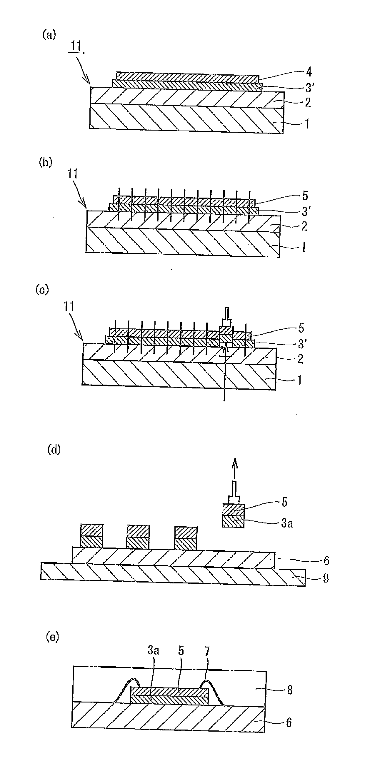
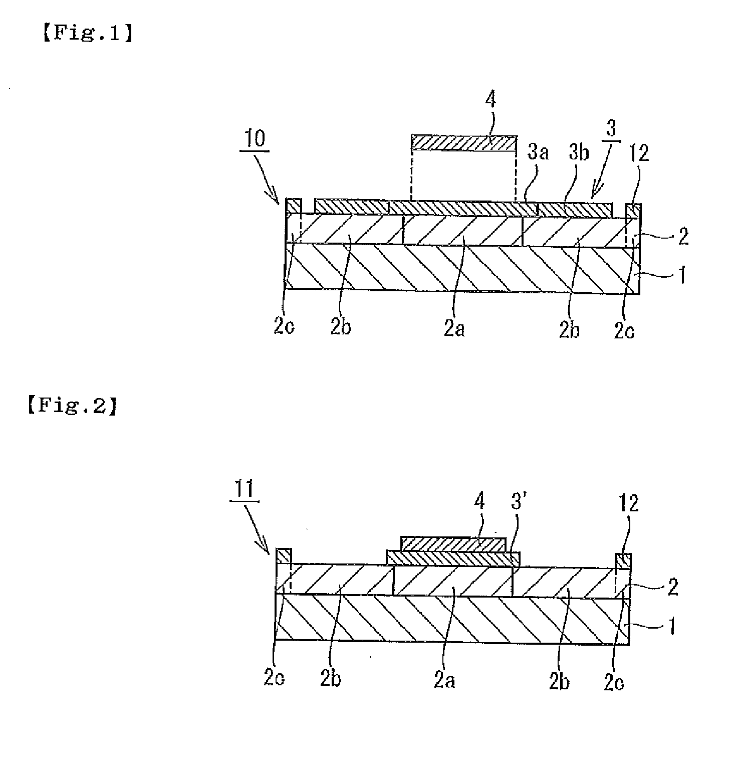
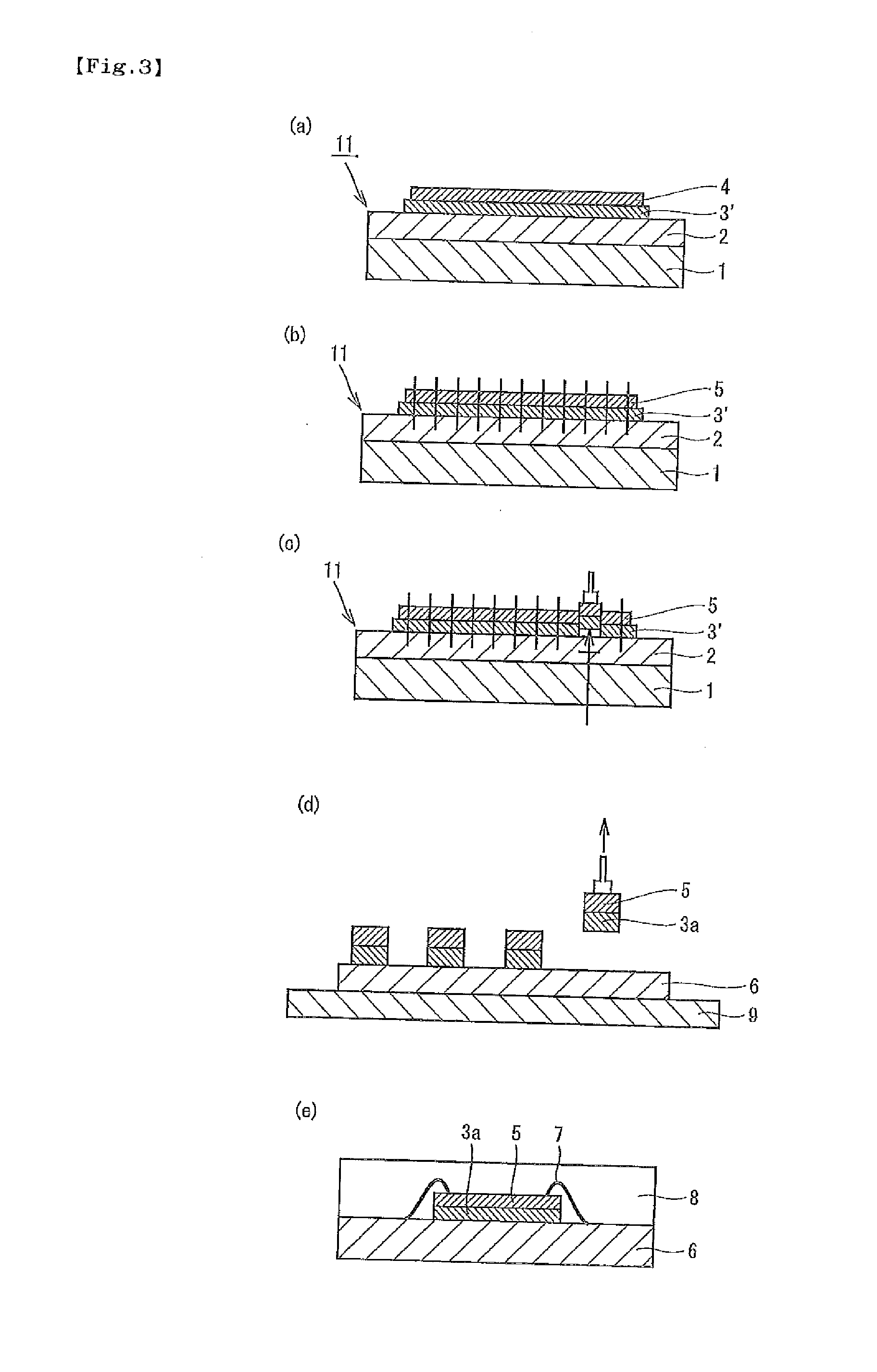
Manufacture of Dicing Film

[0115]To a reaction vessel equipped with a condenser, a nitrogen introducing tube, a thermometer and a stirrer, 86.4 parts of 2-ethylhexyl acrylate (hereinafter referred to as “2EHA”), 13.6 parts of 2-hydroxyethyl acrylate (hereinafter referred to as “HEA”), 0.2 part of benzoyl peroxide and 65 parts of toluene were charged and then polymerized in a nitrogen gas flow at 61° C. for 6 hours to obtain an acrylic polymer A.

[0116]To this acrylic polymer A, 14.6 parts of 2-methacryloyloxyethyl isocyanate (hereinafter referred to as “MOI”) was added and the mixture was subjected to an addition reaction treatment in an air flow at 50° C. for 48 hours to obtain an acrylic polymer A′.

[0117]A pressure-sensitive adhesive composition solution A was obtained by adding 0.5 parts of a polyisocyanate compound (trade name: Colonate L manufactured by Nippon Polyurethane Industry Co., Ltd.) and 5 parts of a photopolymerization initiator (trade name: Irgacure 651 manufactured by...

example 2

Production of Dicing Film

[0121]A dicing film B was obtained in the same manner as in Example 1 except the added amount of the polyisocyanate compound was changed to 1 part.

[0122]A dicing die bond film B was produced by peeling the peeling liner from the dicing film B and by pasting the die bond film layer of the die bond film A to the portion that was irradiated with an ultraviolet ray at 40±3° C.

example 3

Production of Dicing Film

[0123]A dicing film C was obtained in the same manner as in Example 1 except the added amount of the polyisocyanate compound was changed to 2 parts.

[0124]A dicing die bond film C was produced by peeling the peeling liner from the dicing film C and by pasting the die bond film layer of the die bond film A to the portion that was irradiated with an ultraviolet ray at 40±3° C.


PUM

PropertyMeasurementUnit
tensile speedaaaaaaaaaa
temperatureaaaaaaaaaa
tensile storage modulusaaaaaaaaaa

Abstract

The present invention aims to provide a dicing die bond film that is capable of suppressing peeling of the dicing die bond film from a dicing ring. The present invention provides a dicing die bond film in which the pressure-sensitive adhesive layer contains a polymer formed by performing an addition reaction on a specific acrylic polymer with a specific isocyanate compound, and a specific crosslinking agent, and the specific peeling adhesive power of a portion of the pressure-sensitive adhesive layer where the dicing ring is pasted is 1.0 N / 20 mm tape width or more and 10.0 N / 20 mm tape width or less, the tensile storage modulus at 23° C. of the portion where the dicing ring is pasted is 0.05 MPa or more and less than 0.4 MPa, and the die bond film is pasted to the pressure-sensitive adhesive layer after irradiation with an ultraviolet ray.

Description

BACKGROUND OF THE INVENTION[0001]1. Field of the Invention[0002]The present invention relates to a dicing die bond film, that is used in dicing of a workpiece (semiconductor wafer, etc.) under the condition where an adhesive for fixing a chip-shaped workpiece (semiconductor chip, etc.) and an electrode member is provided on the workpiece before dicing.[0003]2. Description of the Related Art[0004]A semiconductor wafer (workpiece) in which a circuit pattern is formed is diced into semiconductor chips (chip-shaped workpiece) (a dicing step) after the thickness thereof is adjusted as necessary by backside polishing. In the dicing step, the semiconductor wafer is generally washed with an appropriate liquid pressure (normally, about 2 kg / cm2) in order to remove a cutting layer. The semiconductor chip is then fixed onto an adherend such as a lead frame with an adhesive (amounting step), and then transferred to a bonding step. In the mounting step, the adhesive has been applied onto the lea...

Claims


Application Information

Patent Timeline
Patent Type & Authority Applications(United States)
IPC IPC(8): H01L21/78B32B37/02B32B37/14B32B37/06B32B7/12B32B37/12
CPCC09J7/0217C09J133/14Y10T428/2809C09J2205/31C09J2203/326C09J7/385H01L2924/181H01L2224/48091H01L2224/73265H01L2224/83191C09J2301/416H01L21/30
Inventor MURATA, SHUHEIMATSUMURA, TAKESHIYANAGI, YUICHIRO
Owner NITTO DENKO CORP
Why Eureka
Try Eureka