Microfluidic device and manufacturing method thereof

a microfluidic device and manufacturing method technology, applied in the direction of burners, isotope separation, particle separator tubes, etc., can solve the problems of complex, time-consuming and high cost, still needs to be cleared, etc., and achieves the effect of fast and low cost, convenient mass production, and simple structur

Inactive Publication Date: 2009-06-02
IND TECH RES INST
View PDF20 Cites 50 Cited by
  • Summary
  • Abstract
  • Description
  • Claims
  • Application Information

AI Technical Summary

Benefits of technology

[0011]The present invention is directed to a method of manufacturing a microfluidic device having advantages of easy to manufacture, low time-consuming and low cost.
[0014]In the microfluidic device of the present invention, the capillary and the substrate are a unity structure such that the interface between the capillary and the channel is dead-volume free. In addition, the capillary of the microfluidic device is formed with a heating and pulling step, and thus the method is simple, fast and low cost, and it is easy to mass produce.

Problems solved by technology

Although there have been many successes, an important hurdle that still needs to be cleared is the connection between the micro-components of a device and the macro-environment of the world.
The difficulty results from the fact that samples and reagents are typically transferred in quantities of microliters to milliliters whereas microfluidic devices consume only nanoliters or picoliters of samples due to the size of reaction chambers and channels, which have dimensions on the order of microns.
However, these methods disclosed in the above prior references have disadvantages of complex, time consuming and high cost.

Method used


Image

  • Microfluidic device and manufacturing method thereof
  • Microfluidic device and manufacturing method thereof
  • Microfluidic device and manufacturing method thereof

Examples


Embodiment Construction

[0025]Reference will now be made in detail to the present preferred embodiments of the invention, examples of which are illustrated in the accompanying drawings. Wherever possible, the same reference numbers are used in the drawings and the description to refer to the same or like parts.

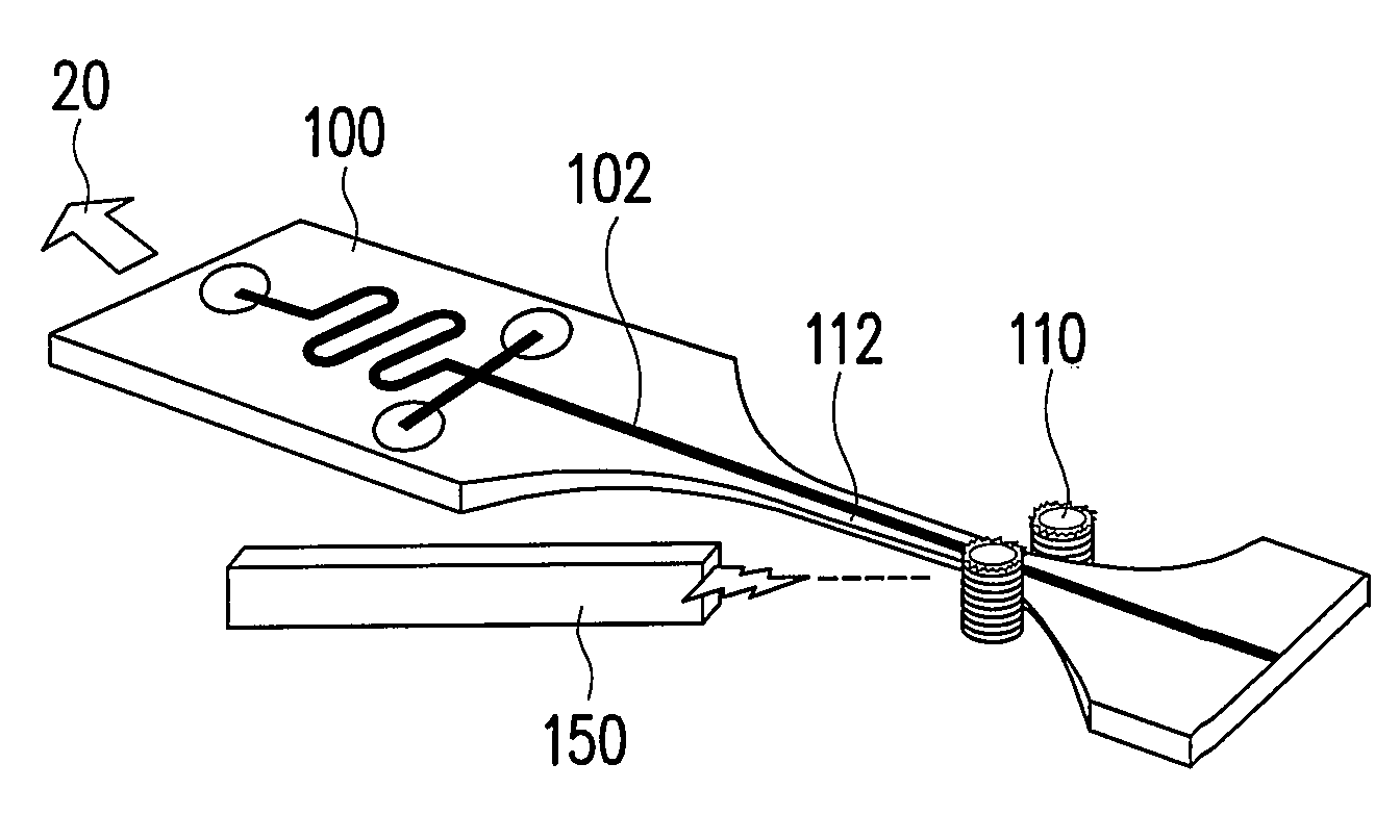
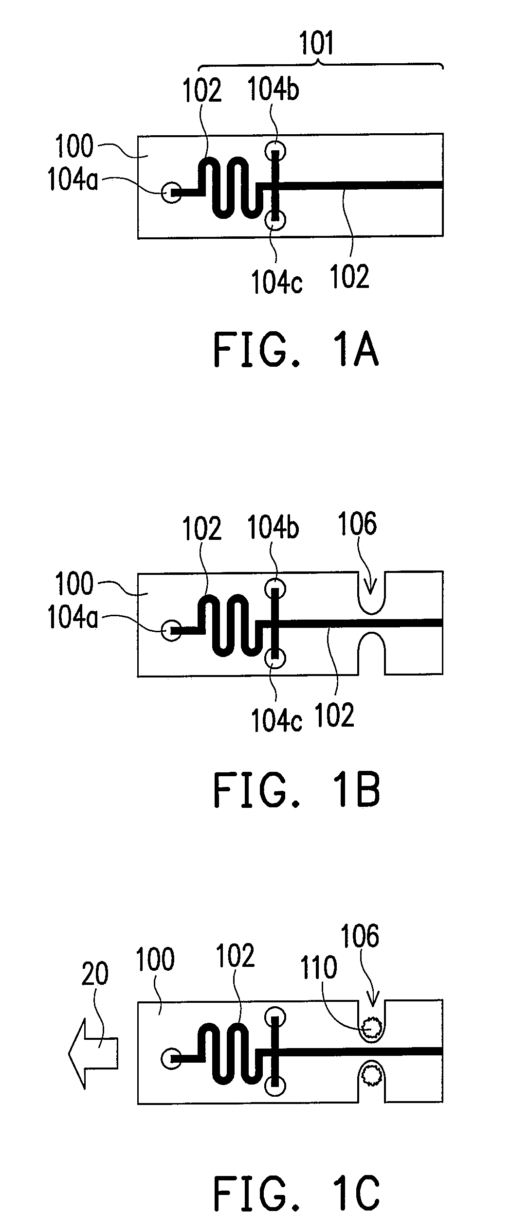
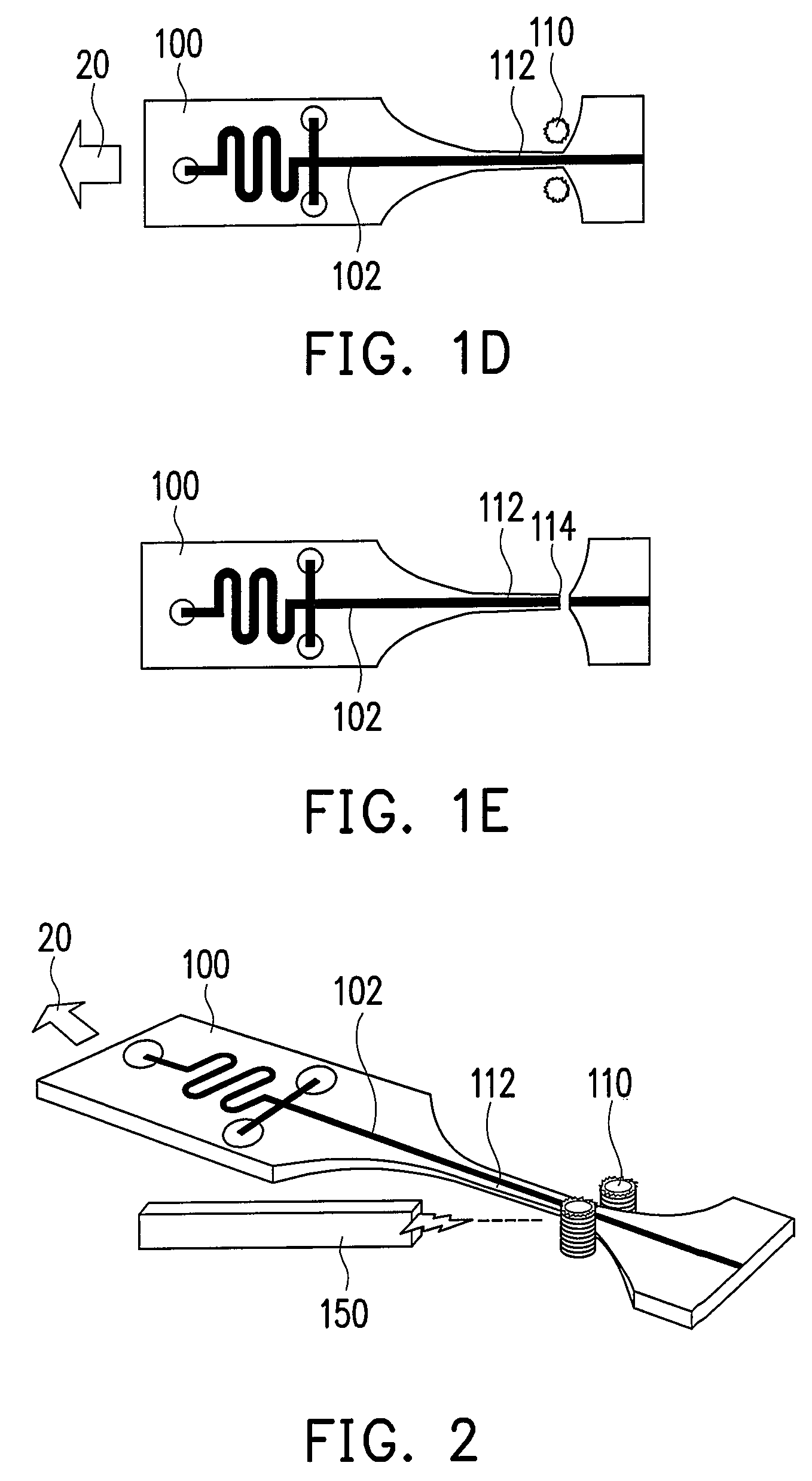
[0026]FIGS. 1A-1E are top views showing a manufacturing method of a microfluidic device according to an embodiment of the present invention. As shown in FIG. 1A, a substrate 100 having at least one device 101 thereon is provided, wherein the device 101 comprises at least one channel 102. In an embodiment, the substrate 100 has a thickness about 0.01˜10 mm, preferably in a range of 0.5˜2 mm, and has a width and length about 1˜5000 μm, preferably in a range of 10-500 μm. The channel 102 of the device 101 may be linear or non-linear, or a portion of the channel 102 is linear and the other portion is non-linear. According to another embodiment, the device 101 formed on the substrate 100 has a plurality o...


PUM

PropertyMeasurementUnit
lengthaaaaaaaaaa
widthaaaaaaaaaa
lengthaaaaaaaaaa

Abstract

A method of manufacturing a microfluidic device is described. A substrate having at least one device thereon is provided, wherein the device includes at least one channel. Next, a region beside the channel is heated, and then the substrate is pulled to neck the region such that at least one capillary connecting with the channel is formed. The present invention also provides a microfluidic device including a substrate and at least one capillary. In particular, the substrate has at least one device thereon, and the device has at least one channel. The capillary is connected with the channel, wherein the substrate and the capillary are a unity structure such that the interface between the capillary and the channel is dead-volume free.

Description

CROSS-REFERENCE TO RELATED APPLICATION[0001]This application claims the priority benefit of U.S.A. provisional application Ser. No. 60753824, filed on Dec. 23, 2005, all disclosures are incorporated therewith. This application also claims the priority of Taiwan application serial no. 95101886, filed Jan. 18, 2006. All disclosure of the Taiwan application is incorporated herein by reference.BACKGROUND OF THE INVENTION[0002]1. Field of the Invention[0003]The present invention generally relates to a microfluidic device and a manufacturing method thereof. More particularly, the present invention relates to a microfluidic device with at least a capillary having dead-volume free interface therebetween.[0004]2. Description of Related Art[0005]Since the concept of miniaturized total analysis systems are developed, a great number of microfluidic devices have been demonstrated for a variety of applications. Common analytical assays including polymerase chain reaction (PCR), DNA analyses and s...

Claims


Application Information

Patent Timeline
Patent Type & Authority Patents(United States)
IPC IPC(8): B01L3/02H01J49/04
CPCB01L3/502707B29C55/04H01J49/0018H01J49/165Y10T29/49432B01L2200/12B01L2300/0816B01L2300/0838B01L2300/0887B01L2400/0406B29L2031/756A61B5/1411A61B10/0045A61B10/007A61B2017/00526B01L2200/027A61B5/150022A61B5/150251A61B5/150274A61B5/150358
Inventor WENG, KUO-YAO
Owner IND TECH RES INST
Why Eureka
Try Eureka