Light emitting display

a technology of light-emitting displays and aperture ratios, which is applied in the field of light-emitting displays, can solve the problems of the deterioration of the aperture ratio of the light-emitting display due to the emission control line, and achieve the effects of reducing the size of the data driving part, minimizing color breakage, and improving the aperture ratio

Active Publication Date: 2009-06-02
SAMSUNG DISPLAY CO LTD
View PDF13 Cites 25 Cited by
  • Summary
  • Abstract
  • Description
  • Claims
  • Application Information

AI Technical Summary

Benefits of technology

[0014]Accordingly, an embodiment of the present invention provides a pixel and a light emitting display using the same, in which threshold voltages of transistors are compensated so that a uniform current for uniform brightness flows to an organic light emitting diode (OLED) in spite of a deviation in the threshold voltages. An embodiment of the present invention provides a plurality of OLEDs and a light emitting display using the same that emit light through one pixel circuit so that the embodiment can reduce the number of pixel circuits of the light emitting display, the number of data lines, and the number of pixel power source lines, to reduce the size of a data driving part, and to thus improve aperture ratio. An embodiment of the present invention provides a pixel and a light emitting display using the same capable of controlling points of emission time of a plurality of the OLEDs to minimize color breakup.

Problems solved by technology

Also, since one emission control line needs to be connected with a pixel row, the aperture ratio of the light emitting display deteriorates due to the emission control line.

Method used


Image

  • Light emitting display
  • Light emitting display
  • Light emitting display

Examples


first embodiment

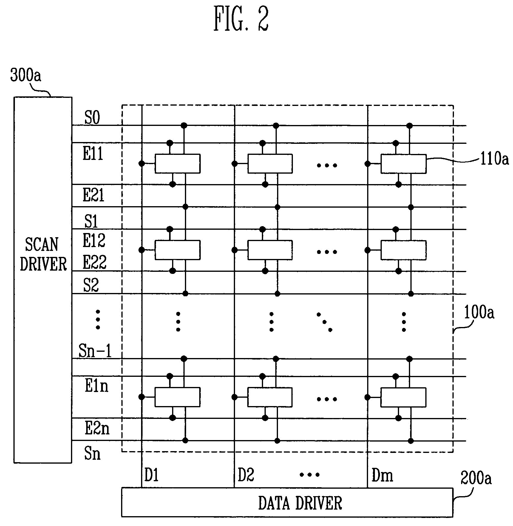
[0036]FIG. 2 illustrates a structure of a light emitting display of the present invention. Referring to FIG. 2, the light emitting display includes an image display unit 100a, a data driver 200a, and a scan driver 300a.

[0037]The image display unit 100a includes a plurality of scan lines S0, S1, S2, . . . , Sn−1, and Sn arranged in a row direction, a plurality of first emission control lines E11, E12, . . . , E1n−1, and E1n and a plurality of second emission control lines E21, E22, . . . , E2n−1, and E2n arranged in the row direction, a plurality of data lines D1, D2, . . . , Dm−1, and Dm arranged in a column direction, a plurality of pixel power source lines (not shown) for supplying pixel power from a pixel power source, and a plurality of pixel circuits 110a. In the present embodiment, first and second OLEDs (not shown) are connected with each pixel circuit 110a.

[0038]Scan signals, data signals, and the pixel power transmitted from the scan lines S0, S1, S2, . . . , Sn−1, and Sn...

second embodiment

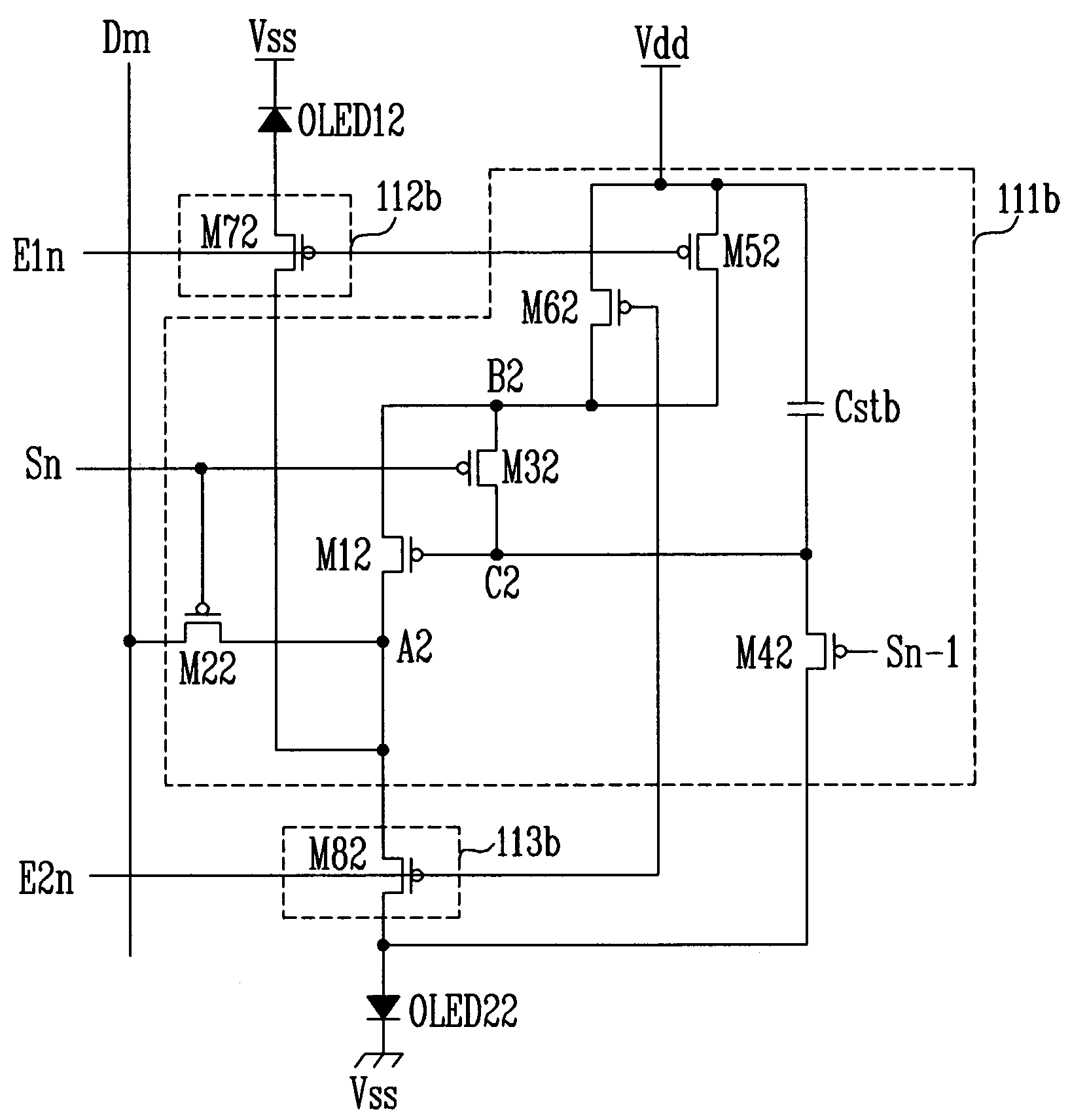
[0056]FIG. 4 is a circuit diagram illustrating a pixel of the light emitting display of FIG. 2. Referring to FIG. 4, the pixel includes a pixel circuit and OLEDs.

[0057]The pixel circuit includes a driving circuit 111b, a first switching circuit 112b, and a second switching circuit 113b. The driving circuit 111b includes first, second, third, fourth, fifth, and sixth transistors M12, M22, M32, M42, M52, and M62 and a capacitor Cstb. The first switching circuit 112b includes a seventh transistor M72. The second switching circuit 113b includes an eighth transistor M82. Each transistor includes a source, a drain, and a gate. The capacitor Cstb includes a first electrode and a second electrode.

[0058]Since the drains and the sources of the first to eighth transistors M12 to M82 have no physical difference, each source and drain may be referred to as a first electrode and a second electrode.

[0059]The drain of the first transistor M12 is connected with a first node A 2, the source of the fi...

third embodiment

[0091]FIG. 10 illustrates a structure of a light emitting display according to the present invention. Referring to FIG. 10, the light emitting display includes an image display unit 100c, a data driver 200c, and a scan driver 300c.

[0092]The image display unit 100c includes a plurality of pixel circuits 110c, four OLEDs (not shown) connected with each of the pixel circuits 110c, a plurality of scan lines S0, S1, S2, . . . , Sn−1, and Sn arranged in a row direction, a plurality of first emission control lines E11, E12, . . . , E1n−1, and E1n, second emission control lines E21, E22, . . . , E2n−1, and E2n, third emission control lines E31, E32, . . . , and E3n-1, and E3n, and fourth emission control lines E41, E42, . . . , E4n−1, and E4n arranged in the row direction, a plurality of data lines D1, D2, . . . , Dm−1, and Dm arranged in a column direction, and a plurality of pixel power source lines (not shown) for supplying pixel power. The pixel power source lines receive the pixel pow...


PUM


Abstract

A light display includes scan lines arranged in a row direction to transmit scan signals, a data line arranged in a column direction to transmit a data signal, an image display unit including emission control lines arranged in the row direction to transmit emission control signals, and a pixel in a region defined by the scan lines and the data line. The pixel has a driving circuit for receiving the signals, the data signal, the emission control signals, and a power to drive a current, a switching circuit connected with the driving circuit to receive the current, the switching circuit for selectively applying the current in accordance with the emission control signals, and organic light emitting diodes (OLEDs) positioned on different rows of the image display unit and connected with the switching circuit to receive the current in accordance with an operation of the switching circuit and to emit light.

Description

CROSS-REFERENCE TO RELATED APPLICATIONS[0001]This application claims priority to and the benefit of Korean Patent Application Nos. 10-2004-95979 and 10-2004-95980, filed on Nov. 22, 2004, in the Korean Intellectual Property Office, the entire contents of which are incorporated herein by reference.BACKGROUND[0002]1. Field of the Invention[0003]The present invention relates to a light emitting display, and more particularly, to a light emitting display capable of compensating for threshold voltages of transistors and capable of having a plurality of organic light emitting diodes (OLED) that emit light through one pixel circuit.[0004]2. Discussion of Related Art[0005]Recently, various flat panel displays having weight and volume less than comparable cathode ray tube (CRT) displays have been developed. In particular, light emitting displays having high luminous efficiency, high brightness, wide view angle, and high response speed are in the limelight[0006]An organic light emitting diode...

Claims


Application Information

Patent Timeline
Patent Type & Authority Patents(United States)
IPC IPC(8): G09G3/32
CPCG09G3/3233G09G3/3291G09G2300/0465G09G2300/0804G09G2300/0814G09G2300/0842
Inventor PARK, SUNG CHEONKWAK, WON KYU
Owner SAMSUNG DISPLAY CO LTD
Why Eureka
Try Eureka