
System and method for performing multi-rank command scheduling in DDR SDRAM memory systems

a memory system and command scheduling technology, applied in the field of ddr sdram memory systems, can solve the problems of increasing the difficulty of achieving maximum sustainable bandwidth, not addressing the issue of data bus synchronization and power limit constraints in ddrx sdram memory systems, and studies offering specific algorithms, so as to minimize bandwidth impact and optimize bandwidth utilization

Inactive Publication Date: 2009-06-02
UNIV OF MARYLAND
View PDF1 Cites 13 Cited by
  • Summary
  • Abstract
  • Description
  • Claims
  • Application Information

AI Technical Summary

Benefits of technology

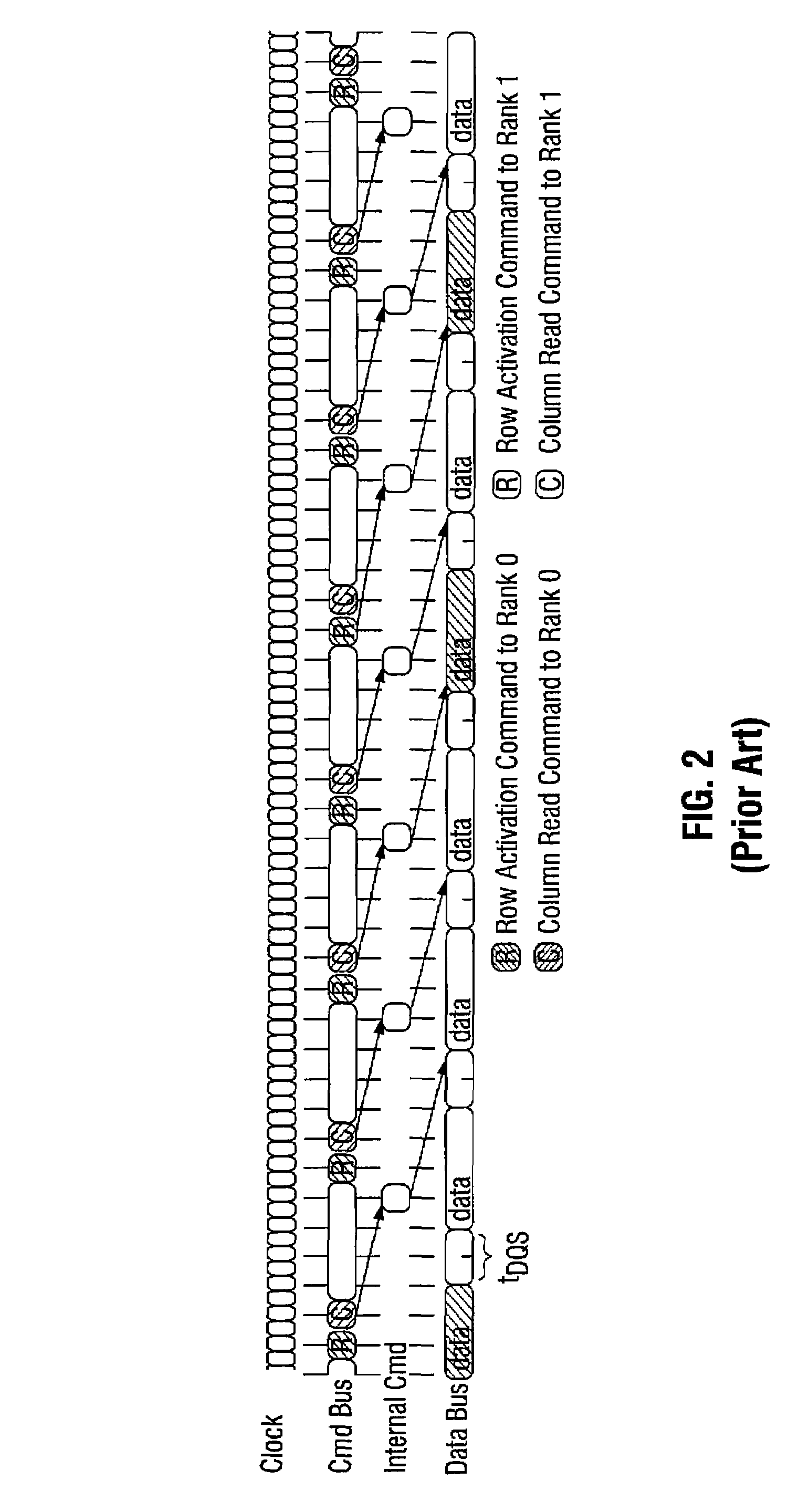
"The present patent provides a memory transaction and DRAM command scheduling algorithm that optimizes bandwidth utilization in a multi-rank DDRx SDRAM memory system while respecting timing constraints. The algorithm selects memory transactions based on their addresses and sequences them in a specific order to minimize the impact of industry standard timing parameters. The algorithm increases the maximum sustainable bandwidth by 41% compared to a moderate system and potentially improves the performance of bandwidth-intensive workloads up to 40%. The algorithm is executed by a memory controller and includes decoupling row access commands and column access commands, scheduling them to different ranks of memory, and group scheduling them to each bank of a given rank."

Problems solved by technology

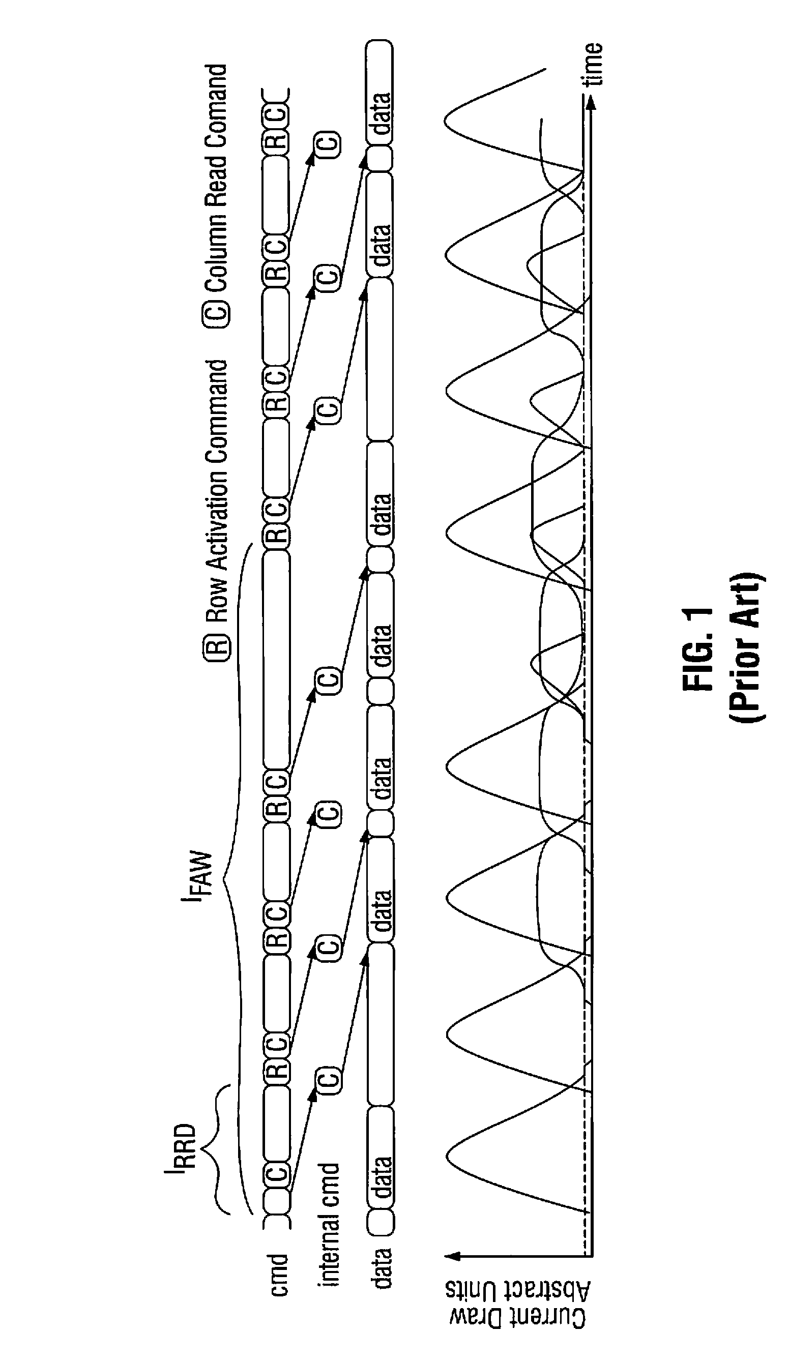
However, constraints such as data bus synchronization overhead in DDRx SDRAM devices memory systems, where x is an integer greater than or equal to two, and constraints that limit peak power in DDR2 and DDR3 devices will significantly impact sustainable bandwidth in high performance DDRx SDRAM memory systems.
Collectively, these trends increase the difficulty of achieving maximum sustainable bandwidth from each successive generation of higher datarate DDRx SDRAM devices by increasing the ratio of DRAM row cycle time to data transport time.
Previous studies have recognized and examined the importance of DRAM access scheduling but do not address the issue of data bus synchronization and power limiting constraints in DDRx SDRAM memory systems.
Previous work in the area of DRAM command scheduling examines the impact of data bus synchronization overhead, write-to-read turnaround times and row-to-row activation times, but does not address the four-bank-activation window limitation of tFAW, nor do any previous studies offer specific algorithms that deal with the conflicting requirements of these different overheads.

Method used


Image

  • System and method for performing multi-rank command scheduling in DDR SDRAM memory systems
  • System and method for performing multi-rank command scheduling in DDR SDRAM memory systems
  • System and method for performing multi-rank command scheduling in DDR SDRAM memory systems

Examples


Embodiment Construction

[0017]To design a high performance DDRx SDRAM memory controller in accordance with the principles of the present disclosure, the issue of memory access scheduling is first discussed to address the constraints imposed on DDR2 and DDR3 SDRAM memory systems by the data bus synchronization overhead of tRTRS and peak power limiting timing parameters tFAW and tRRD. tRTRS is a timing parameter that represents the data strobe signal hand-off time. The single parameter tRTRS accounts for data strobe post-amble time tRPST and the data strobe pre-amble time tRPRE. The timing parameters tFAW, tRRD, tRPST and tRPRE are industry standard timing parameters that can be found in DRAM device datasheets. Following the discussion of memory access scheduling, the DRAM transaction and command scheduling algorithm according to the present disclosure is described, and the maximum sustainable bandwidth of the algorithm is illustrated.

A. Preliminary Information

A.1. Row Buffer Management Policy

[0018]Previous ...


PUM


Abstract

A DRAM command scheduling algorithm is presented that is designed to alleviate various constraints imposed upon high performance, high datarate, short channel DDRx SDRAM memory systems. The algorithm amortizes the overhead costs of rank-switching time and schedules around the tFAW bank activation constraint. A multi-rank DDRx memory system is also presented having at least two ranks of memory each having a number of banks and at least one memory controller configured for performing the hardware-implemented step of DRAM command scheduling for row access commands and column access commands. The step of command scheduling includes decoupling the row access commands from the column access commands; alternatively scheduling the decoupled row access commands to different ranks of memory; and group scheduling the decoupled column access commands to each bank of the number of banks of a given rank of the different ranks of memory.

Description

PRIORITY[0001]This application claims priority from a United States Provisional Application filed on Apr. 18, 2005 and assigned U.S. Provisional Application Ser. No. 60 / 672,364; the entire contents of which are incorporated herein by reference.BACKGROUND[0002]1. Technical Field[0003]The disclosure relates to DRAM memory systems. In particular, the disclosure relates to command scheduling in DDR SDRAM memory systems.[0004]2. Description of the Prior Art[0005]The primary goal in the design of high performance memory systems is to obtain maximum bandwidth with low request access latencies. However, constraints such as data bus synchronization overhead in DDRx SDRAM devices memory systems, where x is an integer greater than or equal to two, and constraints that limit peak power in DDR2 and DDR3 devices will significantly impact sustainable bandwidth in high performance DDRx SDRAM memory systems. Moreover, while DRAM device datarate increases with each new generation of DDRx SDRAM device...

Claims


Application Information

Patent Timeline
Patent Type & Authority Patents(United States)
IPC IPC(8): G06F12/02
CPCG11C7/1066G11C7/1072G11C7/22G11C11/4076G11C11/4087G06F12/0207G06F12/0292
Inventor JACOB, BRUCE L.WANG, DAVID TAWEI
Owner UNIV OF MARYLAND
Learn More