
Catalytic sensor structure

a sensor structure and catalytic technology, applied in the field of nanostructures, can solve the problems of increasing equipment costs, difficult to produce nanostructures with very small diameters and integrated at a high density, and poor yield of nanostructures by such semiconductor processing techniques

Inactive Publication Date: 2009-06-09
CANON KK
View PDF5 Cites 11 Cited by
  • Summary
  • Abstract
  • Description
  • Claims
  • Application Information

AI Technical Summary

Problems solved by technology

However, in these methods, it is difficult to produce nanowires having very small diameters and integrated at a high density.
Fabrication of nanostructures by such semiconductor processing techniques is poor in yield and increases the equipment cost, and thus a method enabling nanostructures to be fabricated easily and with good reproducibility is desired.

Method used


Image

  • Catalytic sensor structure
  • Catalytic sensor structure
  • Catalytic sensor structure

Examples


example 1

[0132]FIGS. 5A, 5B, 5C, 5D, 5E and 5F are a flow chart showing one Example of a method for production of a nanostructure in the present invention as described previously. In this Example, one example of forming a nanostructure having Pt nanowires formed by the following steps (1) to (5) is shown.

[0133](1) Deposition Step 1 (Deposition of Underlayer) (See FIG. 5A)

[0134]As shown in FIG. 5A, a Si substrate 51 was used as a substrate, a Pd thin film 52 with the thickness of 20 nm was formed on the Si substrate 51 by the magnetron sputtering method in this step. The Pd thin film 52 is a catalysts layer for the electroless plating step described below.

[0135](2) Deposition Step 2 (Deposition of AlSi) (See FIG. 5B)

[0136]In this Example, an example of AlSi is shown, but the AlSi part may be replaced with AlGe or AlSiGe.

[0137]As shown in FIG. 5B, an AlSi structure thin film 53 with the thickness of 100 nm having AlSi as a main component was formed on the Pd thin film 52 with the thickness of ...

example 2

[0151]This Example shows one example of forming a nanostructure having Pt nanowires formed by the following steps (1) to (5).

[0152](1) Deposition Step 1 (Deposition of Underlayer), (2) Deposition Step 2 (Deposition of AlSi)

[0153]These steps are same as the steps in Example 1 described above.

[0154](3) Porous Member Forming Step Used by Electroless Plating Solution, (4) Step of Continuous Electroless Plating Steps

[0155]The thin film fabricated in the steps (1) and (2) described above was immersed in a platinum electroless plating solution at 60° C. for 1 hour. The Pt electroless plating solution used here is a plating solution prepared by mixing together 1) 100 mL of Rectroless Pt 100 base solution, 2) 10 mL of 2.8% aqueous ammonia, 3) 2 mL of Rectroless Pt 100 reducing agent and 4) 88 mL of pure water, and the pH of the plating solution is 12.

[0156]This sample was observed by a FE-SEM and as a result, it was found that Pt with the diameter of 5 nm and the height of 100 nm was filled ...

example 3

[0162]This Example shows one example of forming a nanostructure having Pt nanowires formed by the following steps (1) to (5). This Example shows an example in which Pd fine particles are used as a catalyst layer as a method different from the method in which “the Pd thin film fabricated by the magnetron sputtering method is used as a catalyst layer for electroless plating” described in the paragraph (1) Step of depositing Underlayer in Example 1.

[0163](1) Formation of Pd Fine Particles

[0164]A Si substrate was used as a substrate. Pd fine particles were formed on the Si substrate using a sensitive-active method that is generally known. First, the Si substrate was immersed in a SnCl2 solution to adsorb Sn2+ ions on the surface of the substrate. Then, The Si substrate was immersed in a PdCl2 solution, whereby Pd2+ ions were reduced according to the following reaction to deposit active catalyst nuclei on the surface of the substrate.

Sn2++Pd2+→Sn4++Pd

[0165]The following steps, i.e. (2) d...


PUM

PropertyMeasurementUnit
heightaaaaaaaaaa
diameteraaaaaaaaaa
heightaaaaaaaaaa

Abstract

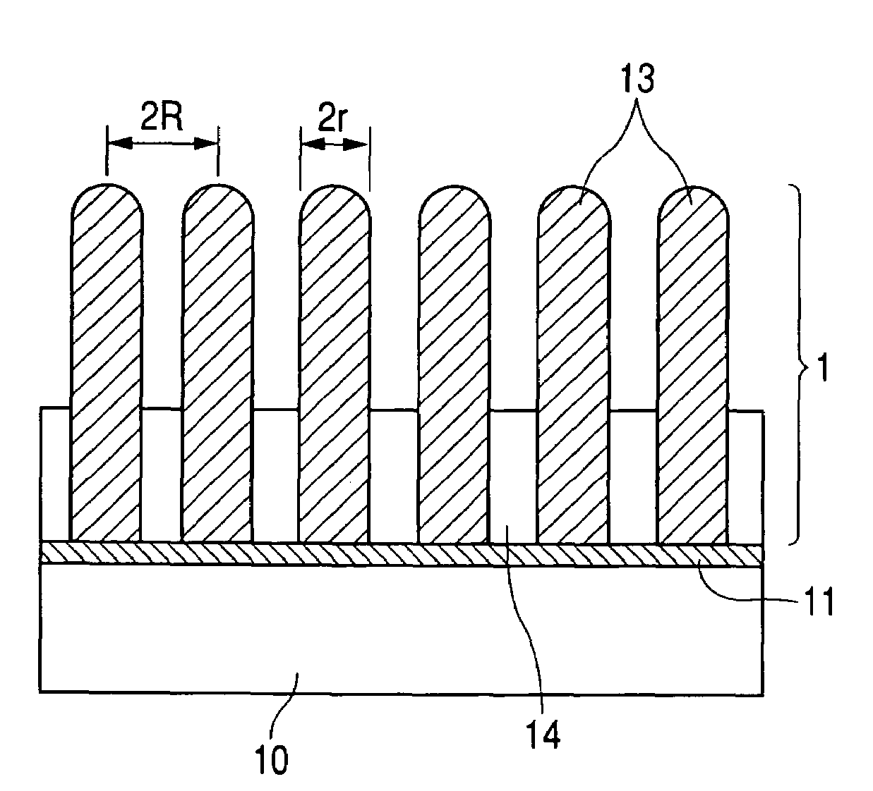
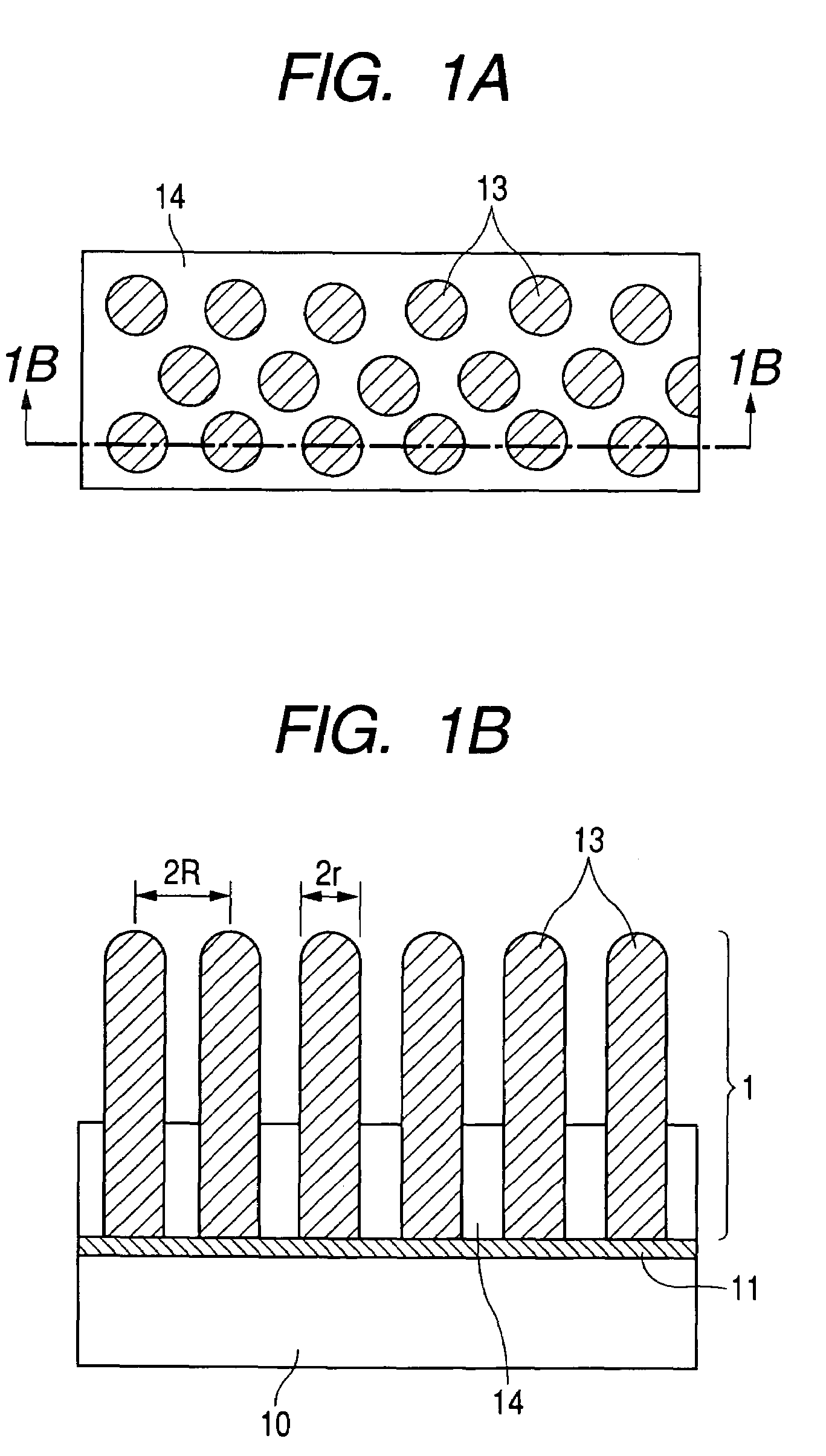
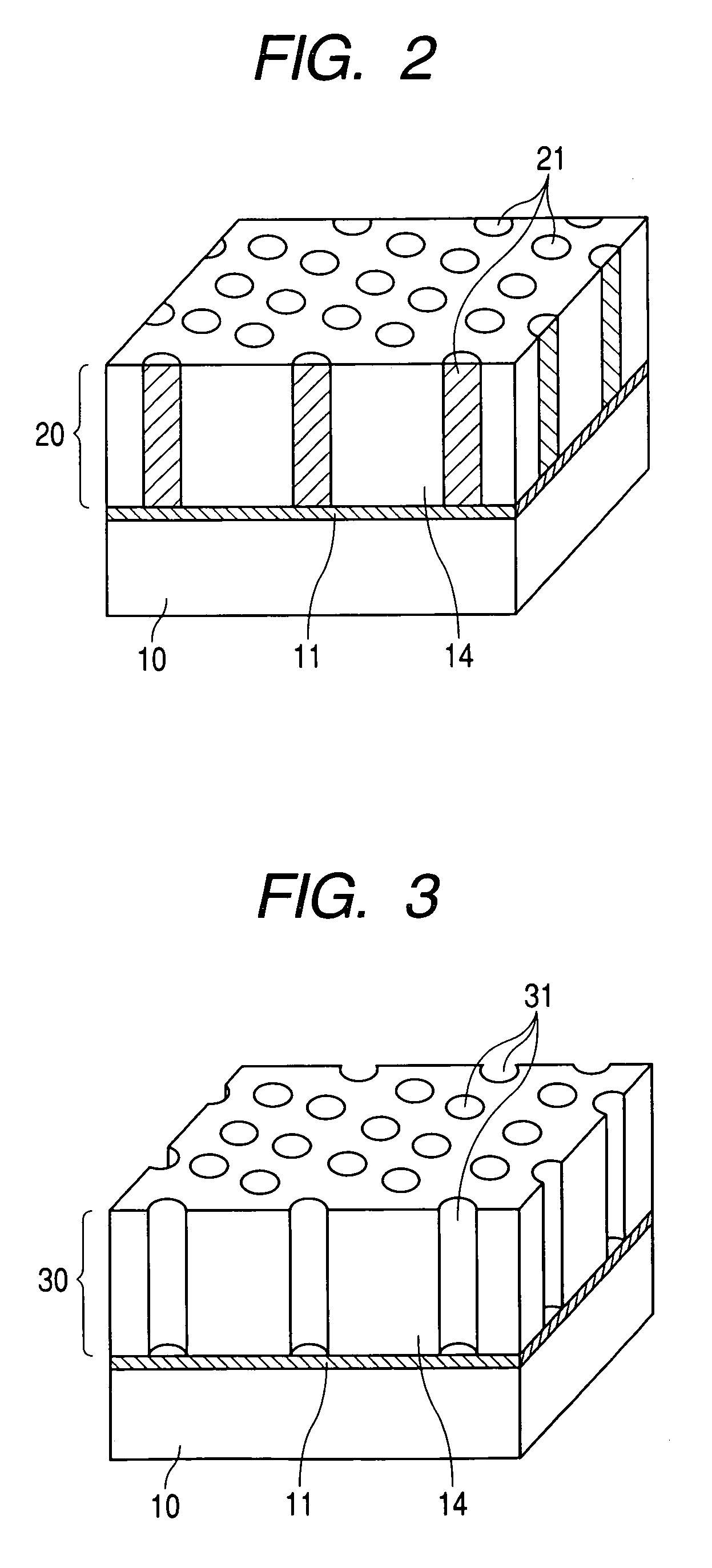
The invention provides a nanostructure including nanowires having very small diameters and integrated at a high density, and capable of being applied to still further high-functional devices.The invention provides a structure including a substrate or substrate having an underlayer, and a structure formed on the substrate or substrate having an underlayer, wherein the structure includes a columnar first part (part) and a second part (part) formed to surround the first part, and the second part comprises two or more types of materials capable of forming eutectic crystals, one type of the materials is a semiconductor material, and the height of the first part from the substrate is greater than the height of the second part from the substrate.

Description

BACKGROUND OF THE INVENTION[0001]1. Field of the Invention[0002]The present invention relates to a nanostructure comprising nanowires vertical or almost vertical to a film face, and a method for production of the same, and particularly to a nanostructure comprising nanowires in which narrow wires having very small diameters are integrated at a high density, characterized in that the average diameter of the nanowires is 20 nm or less, and the length of the nanowire is 1 μm or less. The nanostructure can be used in a wide range as functional materials such as electronic devices and micro-devices, structural materials and the like. Particularly, it can be applied as quantum effect devices, light emitting devices, solar batteries, catalysts, electrochemical sensors, biosensors and the like.[0003]2. Related Background Art[0004]Thin films, narrow wires and dots of metals and semiconductors may exhibit specific electric, optical and chemical natures due to confinement of movement of electr...

Claims


Application Information

Patent Timeline
Patent Type & Authority Patents(United States)
IPC IPC(8): H01L29/43H01L29/06
CPCB82Y10/00H01L29/0665H01L29/0673H01L29/0676Y10S977/778Y10S977/72Y10S977/957Y10S977/78Y10S977/764Y10S977/782
Inventor ICHIHARA, SHIGERUKONAKAHARA, KAORUDEN, TOHRUFUKUTANI, KAZUHIKO
Owner CANON KK
Learn More