Nitride semiconductor device

a technology of nitride and semiconductor devices, which is applied in semiconductor devices, semiconductor/solid-state device details, electrical apparatus, etc., can solve the problems of limited reduction in inability to reduce the size of the electrode pad, and difficulty in ensuring the insulation between the drain electrode pad and the source electrode with a normal interlayer insulating film, so as to achieve a small device area

Active Publication Date: 2009-06-23
PANASONIC CORP
View PDF3 Cites 35 Cited by
  • Summary
  • Abstract
  • Description
  • Claims
  • Application Information

AI Technical Summary

Problems solved by technology

However, since an electrode pad for connecting wirings occupies a large area, the size of the nitride semiconductor device cannot be reduced sufficiently.
It is possible to reduce the size of an electrode pad, but such reduction in size of the electrode pad is limited in view of the yield.
It is therefore difficult to assure insulation between the drain electrode pad and the source electrode with a normal interlayer insulating film.
It is therefore difficult to assure flatness of the electrode pad.

Method used


Image

  • Nitride semiconductor device
  • Nitride semiconductor device
  • Nitride semiconductor device

Examples


first embodiment

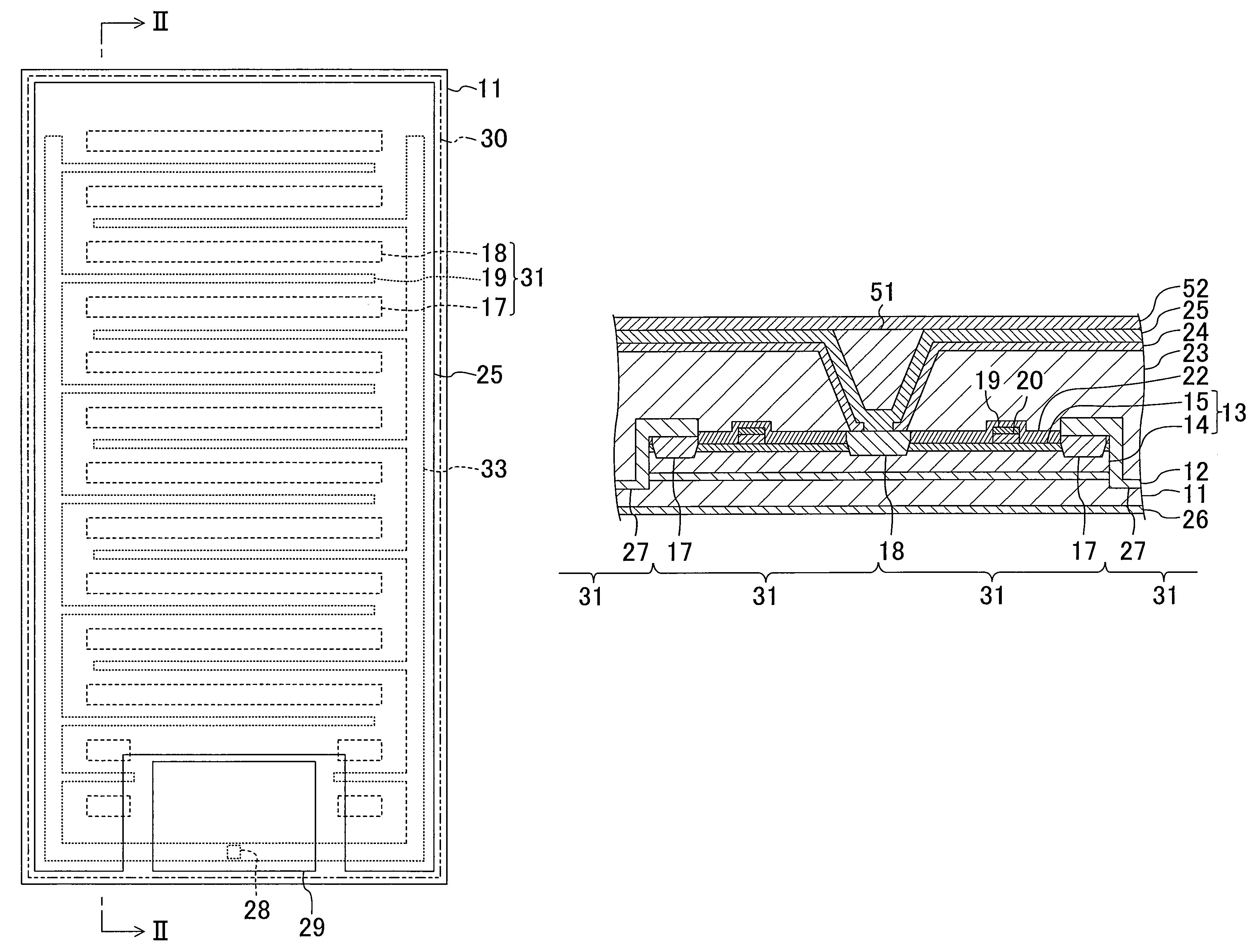
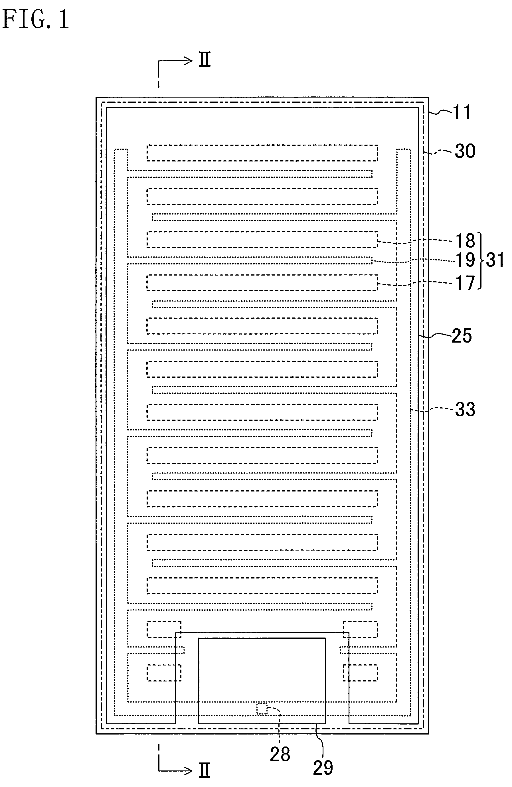
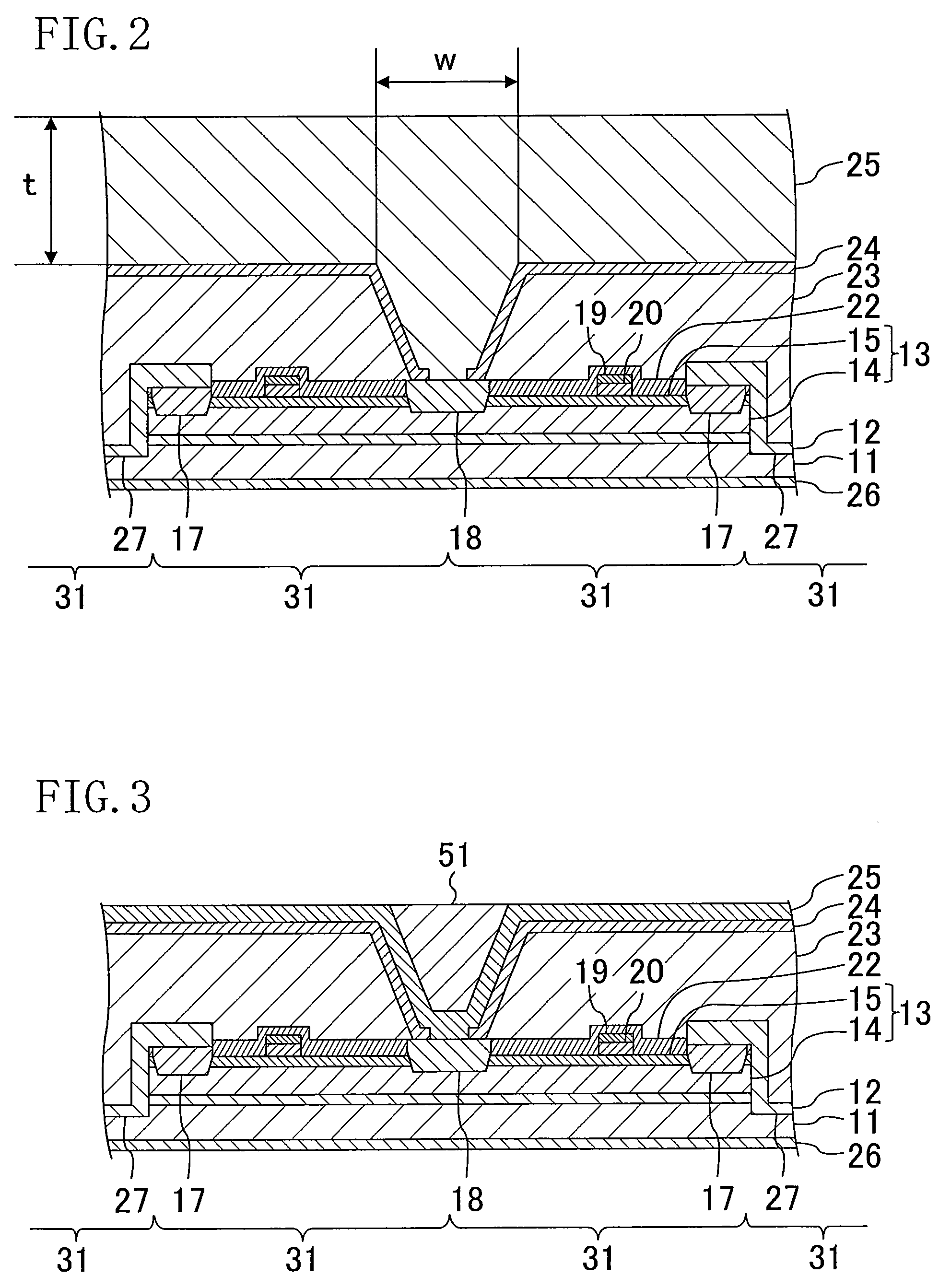
[0023]Hereinafter, a first embodiment of the invention will be described with reference to the accompanying drawings. FIG. 1 shows a planar structure of a nitride semiconductor device of the first embodiment. FIG. 2 shows a cross-sectional structure taken along line II-II in FIG. 1.

[0024]As shown in FIGS. 1 and 2, the nitride semiconductor device of the first embodiment has a nitride semiconductor layer 13 formed on an electrically conductive silicon (Si) substrate 11 with a buffer layer 12 interposed therebetween. The nitride semiconductor layer 13 is formed from an undoped gallium nitride (GaN) layer 14 having a thickness of 2 μm and an undoped aluminum gallium nitride (AlGaN) layer 15 having a thickness of 25 nm. The undoped GaN layer 14 and the undoped AlGaN layer 15 are sequentially formed over the substrate 11 in this order. A two-dimensional electron gas (2DEG) is generated in an interface region of the undoped GaN layer 14 with the undoped AlGaN layer 15, forming a channel r...

second embodiment

[0046]Hereinafter, a second embodiment of the invention will be described with reference to the accompanying drawings. FIG. 6 shows a planar structure of a nitride semiconductor device according to the second embodiment. FIG. 7 shows a cross-sectional structure taken along line VII-VII of FIG. 6.

[0047]As shown in FIGS. 6 and 7, the nitride semiconductor device of the second embodiment has a nitride semiconductor layer 63 formed on an electrically conductive silicon (Si) substrate 61 with a buffer layer 62 interposed therebetween. The nitride semiconductor layer 63 is formed from an undoped gallium nitride (GaN) layer 64 having a thickness of 2 μm and an undoped aluminum gallium nitride (AlGaN) layer 65 having a thickness of 25 nm. The undoped GaN layer 64 and the undoped AlGaN layer 65 are sequentially formed over the substrate 61 in this order. A two-dimensional electron gas (2DEG) is generated in an interface region of the undoped GaN layer 64 with the undoped AlGaN layer 65.

[0048...


PUM


Abstract

A nitride semiconductor device includes: a substrate; a nitride semiconductor layer formed on a main surface of the substrate and having a channel region through which electrons drift in a direction parallel to the main surface; and a plurality of first electrodes and a plurality of second electrodes formed spaced apart from each other on an active region in the nitride semiconductor layer. An interlayer insulating film is formed on the nitride semiconductor layer. The interlayer insulating film has openings that respectively expose the first electrodes and has a planarized top surface. A first electrode pad is formed in a region over the active region in the interlayer insulating film and is electrically connected to the exposed first electrodes through the respective openings.

Description

CROSS REFERENCE TO RELATED APPLICATION[0001]This application claims priority under 35 U.S.C. §119 on Patent Application No. 2006-341024 filed in Japan on Dec. 19, 2006, the entire contents of which are hereby incorporated by reference. The entire contents of Patent Application No. 2007-268772 filed in Japan on Oct. 16, 2007 are also incorporated by reference.BACKGROUND OF THE INVENTION[0002]1. Field of the Invention[0003]The invention relates to a nitride semiconductor device. More particularly, the invention relates to a nitride semiconductor device that is used as a power device in, e.g., power supply circuits of household appliances.[0004]2. Background Art[0005]A nitride semiconductor represented by the general formula AlxInyGa1-x-yN (where x≦0, y≦0, and 0≦x+y≦1) is a wide gap semiconductor having a wide band gap. Therefore, this nitride semiconductor has a higher breakdown field and a higher saturated electron drift velocity as compared to a compound semiconductor such as galliu...

Claims


Application Information

Patent Timeline
Patent Type & Authority Patents(United States)
IPC IPC(8): H01L29/20
CPCH01L24/05H01L29/7786H01L21/76831H01L2924/1305H01L2924/1306H01L2924/01033H01L2924/01023H01L2924/01006H01L2924/13091H01L2924/13055H01L29/2003H01L29/4175H01L2224/05624H01L2224/05647H01L2924/01004H01L2924/01013H01L2924/01014H01L2924/01022H01L2924/01029H01L2924/01046H01L2924/0105H01L2924/01074H01L2924/01079H01L2924/10329H01L2924/00014H01L2924/00H01L29/1066H01L23/4824
Inventor SHIBATA, DAISUKENAKAZAWA, KAZUSHIHIKITA, MASAHIROUEMOTO, YASUHIROUEDA, TETSUZOYANAGIHARA, MANABUTANAKA, TSUYOSHI
Owner PANASONIC CORP
Why Eureka
Try Eureka