Laser irradiation apparatus, laser irradiation method and method for manufacturing semiconductor device

a laser irradiation and laser irradiation technology, applied in laser beam welding apparatus, lasers, manufacturing tools, etc., can solve the problems of low conversion efficiency into harmonic using non-linear optical elements, low density of photon to time, and much lower resistance of non-linear optical elements to laser light, etc., to achieve the effect of reducing the proportion of the region, reducing the size of the beam spot, and increasing throughpu

Inactive Publication Date: 2009-06-23
SEMICON ENERGY LAB CO LTD
View PDF45 Cites 32 Cited by
  • Summary
  • Abstract
  • Description
  • Claims
  • Application Information

AI Technical Summary

Benefits of technology

[0014]In view of the above problem, it is an object of the present invention to provide a laser irradiation apparatus that can make the beam spot much larger than a CW laser irradiation apparatus, that can suppress the thermal damage given to the glass substrate, and that can grow the crystal continuously toward the scanning direction so as to form an aggregation of the crystal grains including a single crystal extending long in the scanning direction. Moreover, it is an object of the present invention to provide a laser irradiation apparatus that can suppress the deterioration of the non-linear optical element and that can obtain the laser light having higher power. Furthermore, it is an object of the present invention to provide a laser irradiation method and a method for manufacturing a semiconductor device that use the laser irradiation apparatus.
[0015]The present inventors considered that it is possible to obtain the crystal grain growing continuously toward the scanning direction by oscillating the laser light at the pulse repetition rate that is determined so that the pulsed laser light is irradiated after the semiconductor film is melted by the previous pulsed laser light and before it is solidified. That is to say, the lower limit of the pulse repetition rate is determined so that the pulse period becomes shorter than the period since the semiconductor film is melted until it is solidified.

Problems solved by technology

However, the CW laser has a problem that the resistance of the non-linear optical element against the laser light is much lower than that when using the pulsed laser because the CW laser burdens the non-linear optical element continuously.
Moreover, since the CW laser has lower output power than the pulsed laser per unit time, the density of photon to time is also low, and therefore the conversion efficiency into the harmonic using the non-linear optical element is low.
Therefore, since the harmonic of the CW laser has lower power than that of the pulsed laser per unit time, it is difficult to increase the throughput by enlarging the beam spot of the CW laser.
As thus described, the CW laser is inferior to the pulsed excimer laser in terms of throughput, and this causes low productivity.
Moreover, although the adjustment of the optical system can decrease to some extent the region in which the extremely small crystal grain is formed, this region cannot be eliminated completely.
However, in the case of the CW laser, it is difficult to enlarge the beam spot according to the above reason, and the width of the beam spot of the CW laser is narrower than that of the pulsed laser.
Therefore, the layout of the semiconductor element is restricted.
Therefore, even in the nonequilibrium state, the CW laser is not preferable because the CW laser gives more thermal damage to the glass substrate than the pulsed laser when performing the laser annealing to the semiconductor film over the glass substrate.
When the thermal damage is given too much to the glass substrate, the glass substrate shrinks accordingly.

Method used


Image

  • Laser irradiation apparatus, laser irradiation method and method for manufacturing semiconductor device
  • Laser irradiation apparatus, laser irradiation method and method for manufacturing semiconductor device
  • Laser irradiation apparatus, laser irradiation method and method for manufacturing semiconductor device

Examples


embodiment 1

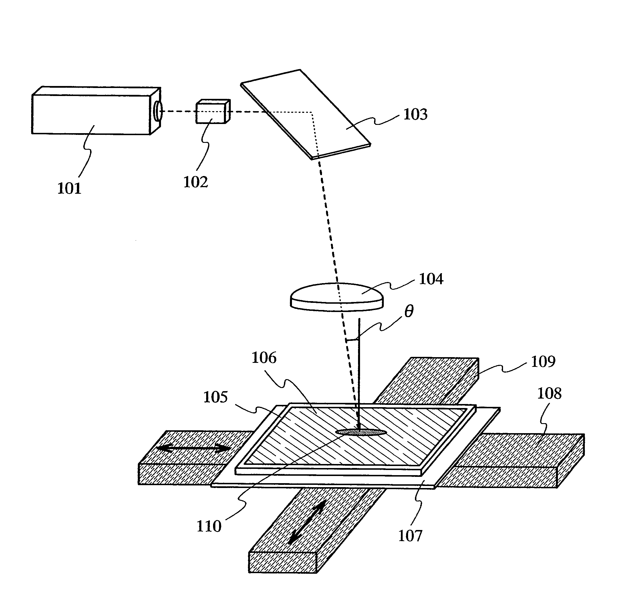
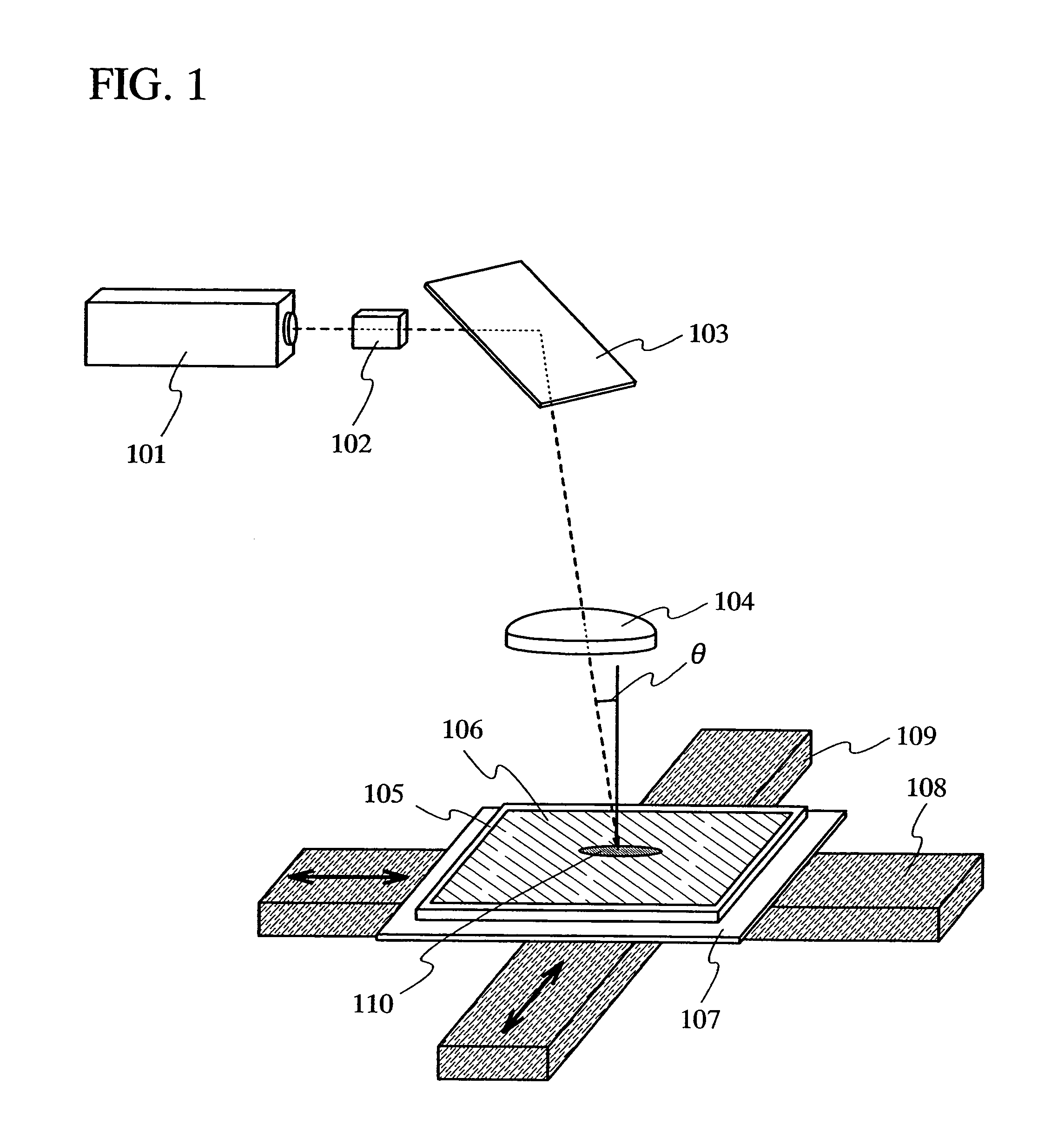
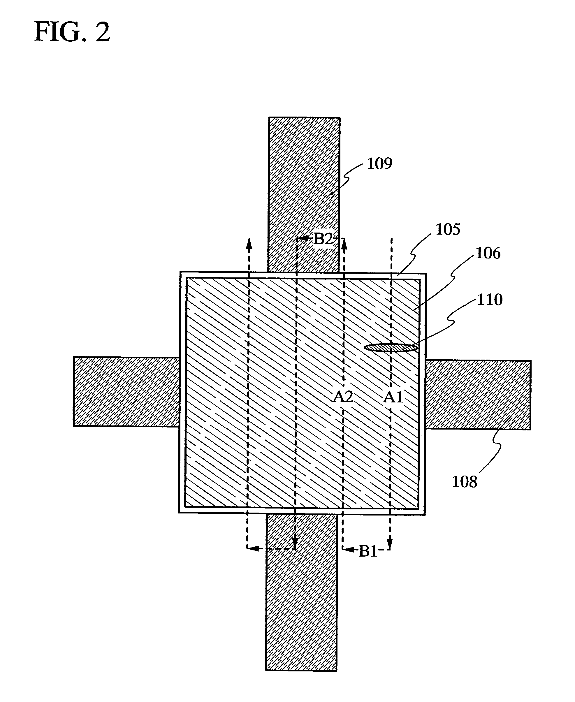
[0059]This embodiment explains an optical system in the laser irradiation apparatus of the present invention with reference to FIGS. 4A and 4B.

[0060]The optical system shown in FIG. 4A has two cylindrical lenses 701 and 702. The beam spot of the laser light incident from the direction indicated by an arrow is shaped by the cylindrical lenses 701 and 702 and then it is irradiated to a processing object 703. It is noted that the cylindrical lens 702 closer to the processing object 703 has a shorter focal length than the cylindrical lens 701.

[0061]When the laser having a pulse width of approximately 10 ps is used according to the present invention, the optical system can be set without considering the effect of the interference. In other words, the laser light may be made incident into the processing object 703 vertically.

[0062]FIG. 4B shows an optical system for combining four beam spots into one beam spot. The optical system shown in FIG. 4B has six cylindrical lenses 717 to 722. The...

embodiment 2

[0068]This embodiment explains a laser irradiation method and a method for manufacturing a semiconductor device of the present invention with reference to FIGS. 5A to 5C.

[0069]Initially, a base film 501 is formed on a substrate 500 as shown in FIG. 5A. A glass substrate such as a barium borosilicate glass or an alumino borosilicate glass, a quartz substrate, a stainless substrate, or the like can be used as the substrate 500 for example. In addition, although a substrate made of flexible synthetic resin such as acrylic or plastic typified by PET, PES, or PEN tends to be inferior to the above substrates in point of the resistance against the heat, the substrate made of flexible synthetic resin can be used when it can resist the heat generated in the manufacturing process.

[0070]The base film 501 is provided in order to prevent the alkali-earth metal or alkali metal such as Na included in the substrate 500 from diffusing into the semiconductor film. The alkali-earth metal or the alkali...

embodiment 3

[0084]Unlike the embodiment 2, this embodiment explains an example in which the crystallization method by the laser irradiation apparatus of the present invention is combined with the crystallization method by the catalyst element.

[0085]Initially, the process up to forming the semiconductor film 502 is performed with reference to FIG. 5A of the embodiment 2. Next, as shown in FIG. 6A, a nickel acetate solution including Ni in the range of 1 to 100 ppm in weight is applied to the surface of the semiconductor film 502 by a spin coating method. It is noted that the catalyst may be added not only by the above method but also by another method such as a sputtering method, a vapor deposition method, or a plasma process. Next, the heat treatment is performed for 4 to 24 hours at temperatures ranging from 500 to 650° C., for example for 14 hours at a temperature of 570° C. This heat treatment forms a semiconductor film 520 in which the crystallization is promoted in the vertical direction f...


PUM

PropertyMeasurementUnit
speedaaaaaaaaaa
scanning speedaaaaaaaaaa
lengthaaaaaaaaaa

Abstract

The object of the present invention is to provide a laser irradiation apparatus being able to enlarge the beam spot to a large degree compared with that of the CW laser, to suppress the thermal damage to the glass substrate, and to form an aggregation of crystal grains including a single crystal extending long in a scanning direction by growing the crystal continuously in the scanning direction. The laser irradiation of the present invention comprises a pulsed laser oscillator, a non-linear optical element for converting the wavelength of the laser light emitted from the pulsed laser oscillator, and an optical system for condensing the laser light whose wavelength is converted on a semiconductor film, wherein the pulsed laser oscillator has a repetition rate in the range of 10 MHz to 100 GHz.

Description

BACKGROUND OF THE INVENTION[0001]1. Field of the Invention[0002]The present invention relates to a laser irradiation apparatus used to crystallize a semiconductor film. Moreover, the present invention relates to a laser irradiation method and a method for manufacturing a semiconductor device that use the laser irradiation apparatus.[0003]2. Related Art[0004]A thin film transistor formed using a poly-crystalline semiconductor film (this thin film transistor is hereinafter referred to as a poly-crystalline TFT) is superior in mobility by two digits or more compared to a TFT formed using an amorphous semiconductor film. Therefore, the poly-crystalline TFT has an advantage that a pixel portion and its peripheral driver circuit of a semiconductor display device can be integrally formed over a same substrate. The poly-crystalline semiconductor film can be formed over an inexpensive glass substrate by using a laser annealing method.[0005]In the lasers, there are a pulsed laser and a contin...

Claims


Application Information

Patent Timeline
Patent Type & Authority Patents(United States)
IPC IPC(8): H01S3/10B23K26/073H01L21/00H01L21/20
CPCB23K26/063B23K26/0639B23K26/0643H01L21/2026B23K26/0665B23K26/0853B23K26/0648B23K26/064B23K26/0622H01L21/02686H01L21/02422H01L21/02488H01L21/02678H01L21/02532H01L21/0242H01L21/02595H01L21/02691H01S3/10
Inventor TANAKA, KOICHIROYAMAMOTO, YOSHIAKI
Owner SEMICON ENERGY LAB CO LTD
Why Eureka
Try Eureka