Semiconductor electrochemical etching processes employing closed loop control

a technology of electrochemical etching and semiconductor wafers, applied in semiconductor/solid-state device testing/measurement, manufacturing tools, electric circuits, etc., can solve the problems of limiting the maximum obtainable thickness of the useful mpsi layer, natural modification of electrochemical etching parameters, and not entirely satisfactory current art methods of electrochemical etching of semiconductors for at least some applications. good quality

Inactive Publication Date: 2009-07-14
LAKE SHORE CRYOTRONICS INC
View PDF18 Cites 3 Cited by
  • Summary
  • Abstract
  • Description
  • Claims
  • Application Information

AI Technical Summary

Problems solved by technology

However, current art methods of electrochemical etching of semiconductors are still not entirely satisfactory for at least some applications.
There exist physical constraints that lead to the natural modification of the electrochemical etching parameters during the electrochemical etching process.
As disclosed in this prior art, changes of the etching parameters over the etching time severely limit the maximum obtainable thickness of the useful MPSi layer.
However, no closed-loop control over the electrochemical etching parameters has been found yet, based on these findings.
The time of IV testing must be carefully optimized in this case since it may cause considerable effect on the results.

Method used


Image

  • Semiconductor electrochemical etching processes employing closed loop control
  • Semiconductor electrochemical etching processes employing closed loop control
  • Semiconductor electrochemical etching processes employing closed loop control

Examples


Embodiment Construction

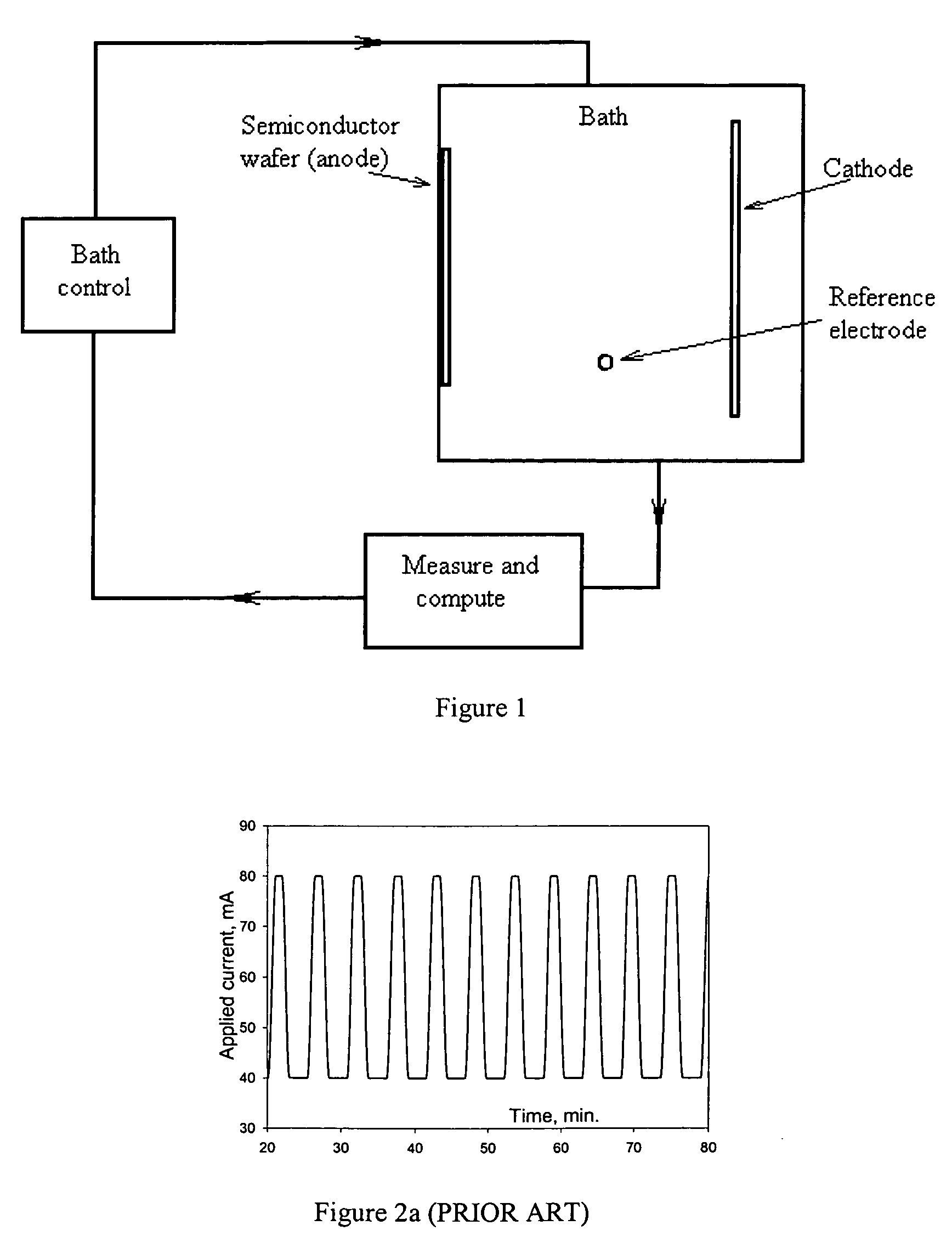
[0039]According to the first exemplary illustrative non-limiting implementation, the closed-loop control over the semiconductor electrochemical etching process can be realized by[0040]measuring the present value of the resistivity (or conductivity) of the semiconductor wafer / electrolyte / electrode electrochemical system[0041]adjusting the electrochemical etching parameters automatically and continuously or quasi-continuously, according to the detected changes in said value of the resistivity (or conductivity) of said electrochemical system occurring during the electrochemical etching process.

[0042]Said electrochemical etching parameters that could be adjusted, in the case of a porous multilayer of varying porosities being formed in said semiconductor wafer, include, but are not limited to, the applied current density, time constant of current modulation, amplitude of said current modulation, and temperature of said electrolyte. The schematic block-diagram of the closed-loop control s...


PUM

PropertyMeasurementUnit
resistivityaaaaaaaaaa
frequencyaaaaaaaaaa
diametersaaaaaaaaaa

Abstract

Methods and apparatus for providing closed-loop control over an electrochemical etching process during porous semiconductor fabrication enhance the quality of the porous semiconductor materials, especially those contained structural variations (such as porosity or morphology variations) along the thickness of said porous semiconductors. Such enhancement of the control over the electrochemical etching process is highly desired for many applications of porous semiconductor materials.

Description

CROSS-REFERENCES TO RELATED APPLICATIONS[0001]This application claims the benefit of provisional application 60 / 537,508 filed Jan. 21, 2004, incorporated herein by reference.STATEMENT REGARDING FEDERALLY SPONSORED RESEARCH OR DEVELOPMENT[0002]Not applicable.FIELD[0003]The technology herein relates to electrochemical or photo-electrochemical etching of semiconductor wafers that employ closed-loop control of pore geometry by detecting changes in the bath etch parameters and utilizing them, or derivations based on them, as closed loop feedback control parameters to obtain desired pore geometry. More particularly, this technology relates to methods of in-situ measurements of etch parameters and methods of extracting information from such measured parameters, and, further, in providing active feedback to the etching system, including changing of the etching parameters according to the results of the in-situ measurements.BACKGROUND AND SUMMARY[0004]Electrochemical etching of semiconductor...

Claims


Application Information

Patent Timeline
Patent Type & Authority Patents(United States)
IPC IPC(8): B23H3/02B23H5/00
CPCC25F3/12H01L21/306H01L21/67253C25F7/00H01L21/67086H01L22/26
Inventor KOCHERGIN, VLADIMIRCHRISTOPHERSEN, MARC
Owner LAKE SHORE CRYOTRONICS INC
Why Eureka
Try Eureka