Optical analog-to-digital converter

an analog-to-digital converter and optical technology, applied in the direction of code conversion, transmission system, instruments, etc., can solve the problems of reducing the accuracy of electronic adcs, limiting the effective number of electronic adcs, and reducing the frequency with increasing frequency

Active Publication Date: 2009-07-21
NAT TECH & ENG SOLUTIONS OF SANDIA LLC
View PDF11 Cites 25 Cited by
  • Summary
  • Abstract
  • Description
  • Claims
  • Application Information

AI Technical Summary

Benefits of technology

[0023]The optical ADC can also optionally include a plurality of semiconductor optical amplifiers located between the optical waveguide splitter for the optical analog signal and the plurality of waveguide photodetectors. The semiconductor optical amplifiers are useful to amplify the N portions of the optical analog signal prior to generating the N photocurrent signals.

Problems solved by technology

The precision of electronic ADCs, however, is currently limited to an effective number of bits (ENOB) of 8.5 at 2 GHz RF bandwidth, and decreases with increasing frequency.

Method used


Image

  • Optical analog-to-digital converter
  • Optical analog-to-digital converter
  • Optical analog-to-digital converter

Examples


Embodiment Construction

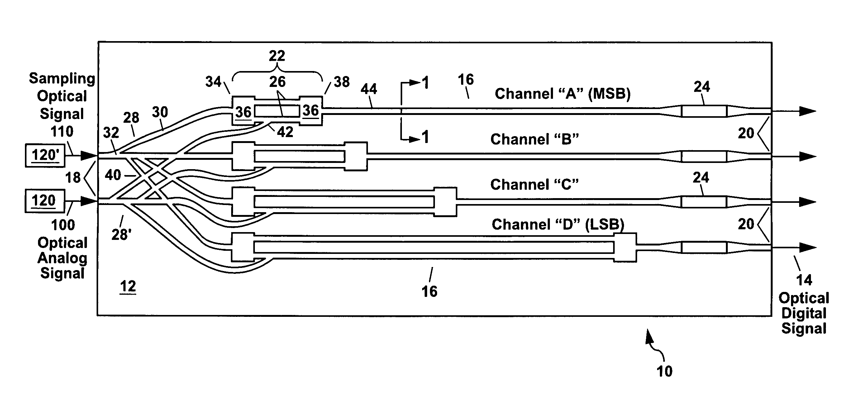
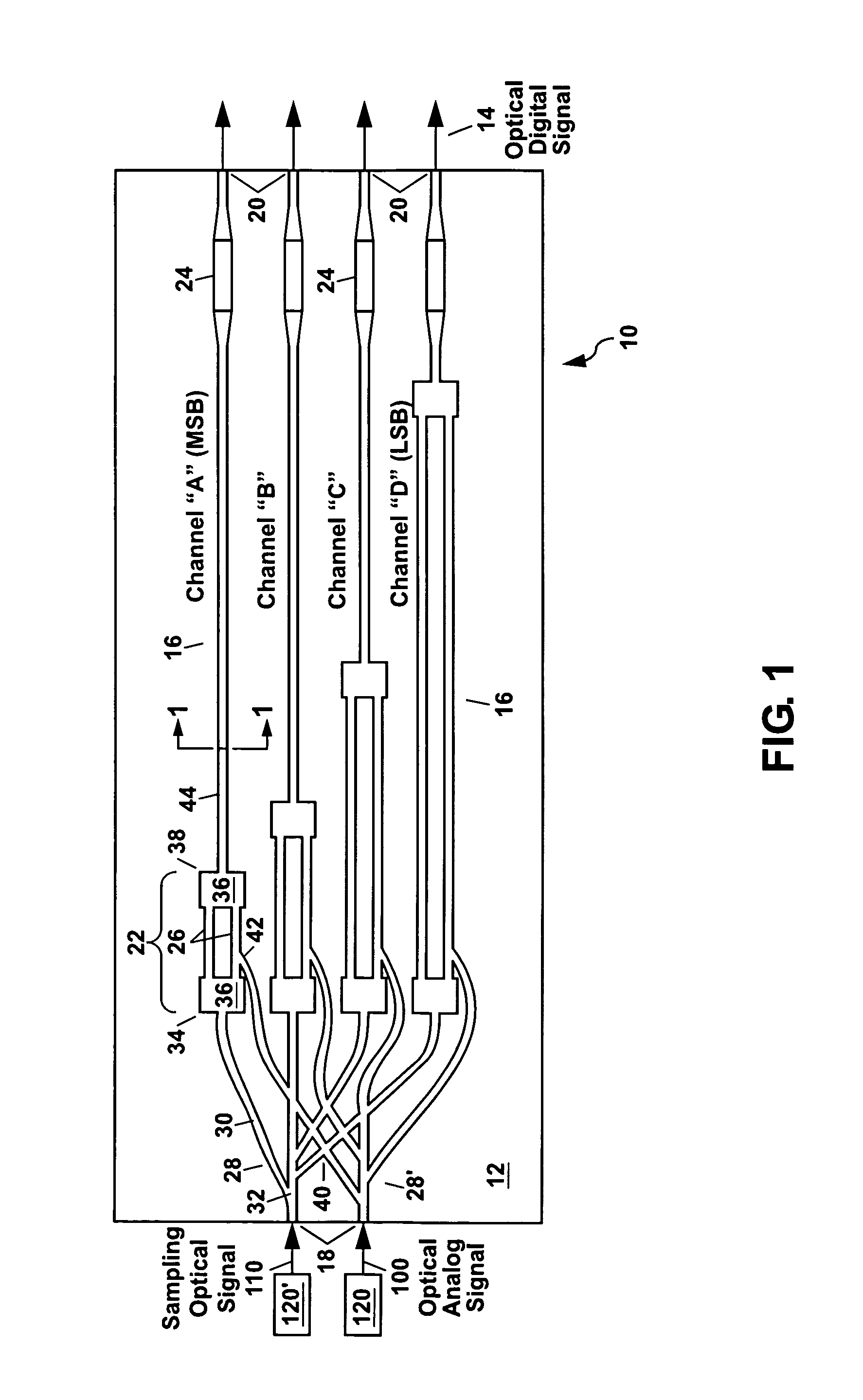
[0036]Referring to FIG. 1, there is shown a schematic plan view of a first example of the optical analog-to-digital converter (ADC) 10 of the present invention. The optical ADC 10, which can be formed as a photonic integrated circuit (PIC) on a common III-V compound semiconductor substrate 12 such as a gallium arsenide (GaAs) substrate or an indium phosphide (InP) substrate, is useful to generate an optical digital signal 14 output which is a digital representation of an optical analog signal 100 which is input to the optical ADC 10. The optical analog signal 100 can be provided, for example, by an optical fiber or a semiconductor laser 120 and can have a radio-frequency (rf) bandwidth from 100 MHz to 10 GHz or more.

[0037]The optical analog signal 100 is sampled and converted to the optical digital signal 14 at a sampling rate which is defined by a sampling optical signal 110 which acts as a clock for the analog-to-digital conversion. The sampling optical signal 110 can be provided ...


PUM


Abstract

An optical analog-to-digital converter (ADC) is disclosed which converts an input optical analog signal to an output optical digital signal at a sampling rate defined by a sampling optical signal. Each bit of the digital representation is separately determined using an optical waveguide interferometer and an optical thresholding element. The interferometer uses the optical analog signal and the sampling optical signal to generate a sinusoidally-varying output signal using cross-phase-modulation (XPM) or a photocurrent generated from the optical analog signal. The sinusoidally-varying output signal is then digitized by the thresholding element, which includes a saturable absorber or at least one semiconductor optical amplifier, to form the optical digital signal which can be output either in parallel or serially.

Description

GOVERNMENT RIGHTS[0001]This invention was made with Government support under Contract No. DE-AC04-94AL85000 awarded by the U.S. Department of Energy. The Government has certain rights in the invention.FIELD OF THE INVENTION[0002]The present invention relates in general to optical analog-to-digital converters (ADCs), and in particular to an optical ADC which can be formed as a photonic integrated circuit (PIC) and which can convert an optical analog input signal into an optical digital output signal.BACKGROUND OF THE INVENTION[0003]Analog-to-digital converters (ADCs) have traditionally been fabricated using electronic integrated circuits. The function of an ADC is to repeatedly sample a time-varying analog waveform, generally at fixed time intervals, and to generate a digital representation of the analog waveform with a certain level of precision. The precision of electronic ADCs, however, is currently limited to an effective number of bits (ENOB) of 8.5 at 2 GHz RF bandwidth, and de...

Claims


Application Information

Patent Timeline
Patent Type & Authority Patents(United States)
IPC IPC(8): H03M1/00
CPCG02F7/00
Inventor VAWTER, G. ALLENRARING, JAMESSKOGEN, ERIK J.
Owner NAT TECH & ENG SOLUTIONS OF SANDIA LLC
Why Eureka
Try Eureka