Integrated circuit having on-chip laser burn-in circuit

a laser burnin circuit and integrated circuit technology, applied in the direction of individual semiconductor device testing, semiconductor lasers, instruments, etc., can solve the problems of eye quality, parasitic addition, and degrade performan

Inactive Publication Date: 2009-07-21
BROADCOM INT PTE LTD
View PDF5 Cites 5 Cited by
  • Summary
  • Abstract
  • Description
  • Claims
  • Application Information

AI Technical Summary

Problems solved by technology

These extra pads add parasitics that degrade performance (e.g., eye quality), particularly for high transmission rates such as 2.5 Gbps or higher.
Furthermore, bonding between the integrated circuit 10 and the digital controller 22 requires a delicate and difficult procedure.
Another drawback to the configuration of FIG. 1 is that the laser driver 16 provides the burn-in current.
Furthermore, using laser driver 16 as the burn-in current source may cause degradation of laser driver 16.
This can result in degradation of laser driver 16.

Method used


Image

  • Integrated circuit having on-chip laser burn-in circuit
  • Integrated circuit having on-chip laser burn-in circuit
  • Integrated circuit having on-chip laser burn-in circuit

Examples


Embodiment Construction

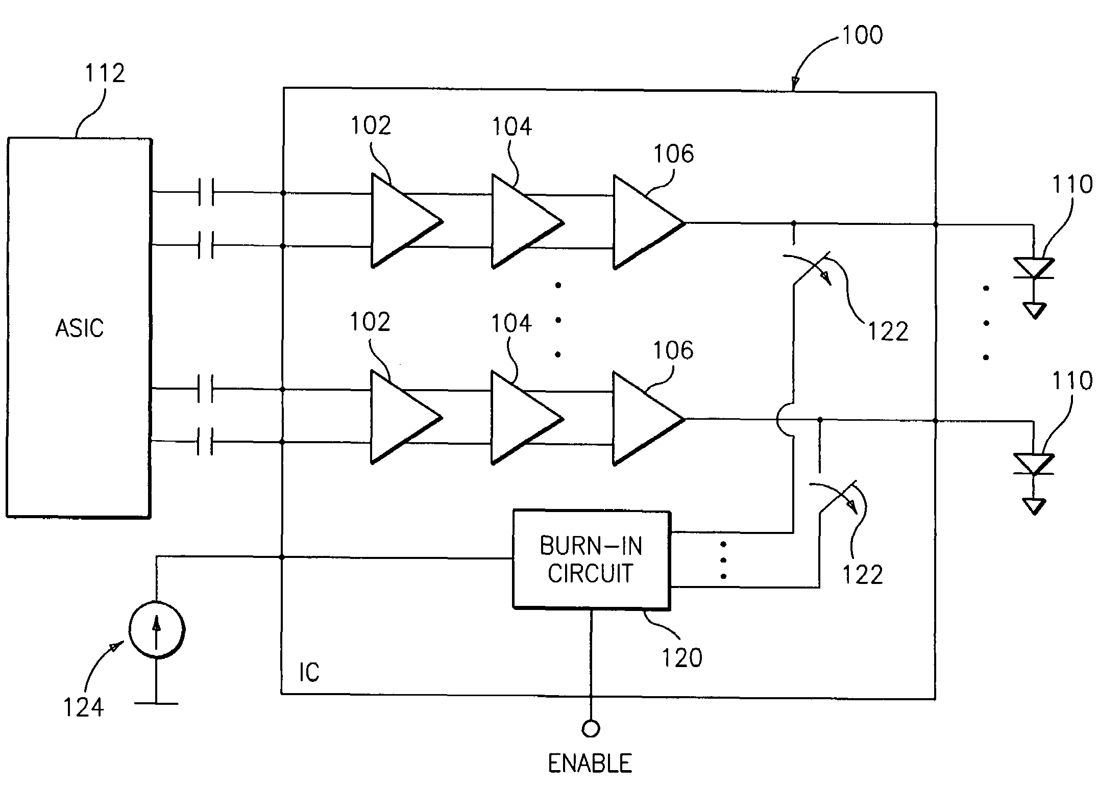
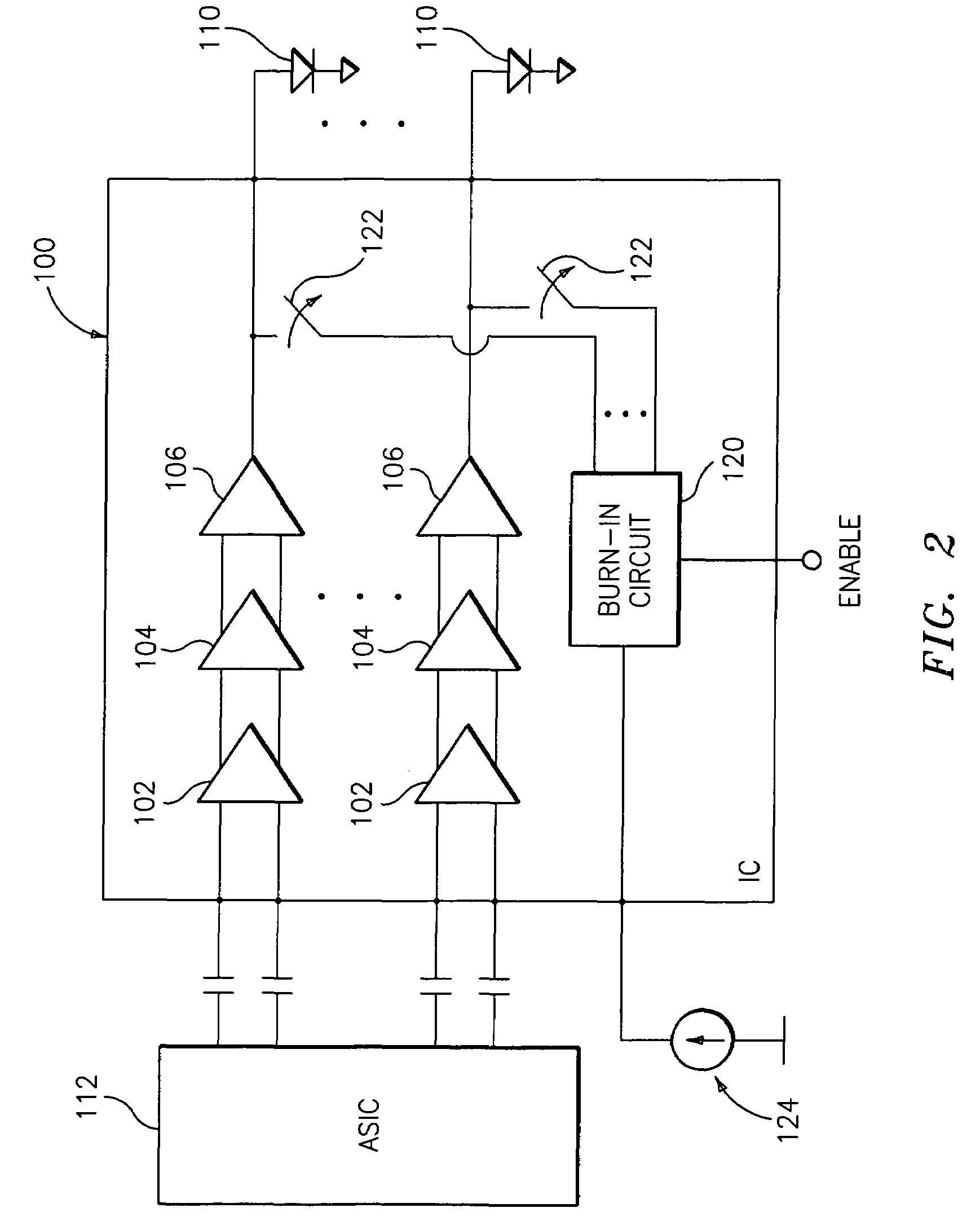
[0012]FIG. 2 is a block diagram of a system for laser diode burn-in in an embodiment of the invention. In FIG. 2, integrated circuit 100 is an N-channel laser drive chip. Each channel includes an input buffer 102, a limiting amplifier 104, and a laser driver 106. Input buffer 102 stores signals from a communication device prior to transmission to the laser driver 106. Limiting amplifier 104 amplifies the output of input buffer 102 and provides the amplified signals to laser driver 106. Laser diver 106 drives laser diode 110 to generate optical signals for communications. An ASIC 112 provides signals to each channel for communications. The laser diodes 110 may be part of a VCSEL in a communications device, such as a fiber optic transmitter.

[0013]Integrated circuit 100 includes a burn-in circuit 120. As described in further detail herein, the burn-in circuit 120 generates burn-in current for the laser diodes 110 during the burn-in process. The burn-in circuit 120 is formed in the inte...


PUM


Abstract

An integrated circuit for providing burn-in current to a laser diode. The integrated circuit includes a laser driver having an output for connection to the laser diode. Burn-in circuitry is formed on the integrated circuit and generates a burn-in current. A switch is formed on the integrated circuit and couples the burn-in current to the laser diode in response to an enable signal.

Description

BACKGROUND[0001]Increasingly, data communications involve transmissions by optical sources that can deliver high volumes of digitized information as pulses of light. This is especially true for many communication companies that utilize laser diodes and optical fibers as their primary means for the transmission of voice, television and data signals for ground-based communications networks.[0002]To achieve high bandwidth, laser diodes such as edge-emitting lasers and Vertical Cavity Surface Emitting Lasers (VCSELs) are commonly utilized as optical sources. These types of laser diodes are preferred due to their minute dimensions. For example, the typical VCSEL is measured in the order of micrometers. Consequently, an array of laser diodes can be integrated into a system to achieve high bandwidth transmissions.[0003]In the manufacturing and production of VCSEL arrays, such as 1×12 or 1×4 parallel channel optical arrays, target optical and electrical characteristics are assigned to the a...

Claims


Application Information

Patent Timeline
Patent Type & Authority Patents(United States)
IPC IPC(8): H01S3/00
CPCH01S5/0261H01S5/0014
Inventor KIM, YOUNG GONLEE, MYUNGHEE
Owner BROADCOM INT PTE LTD
Why Eureka
Try Eureka