
Ink jet head circuit board, method of manufacturing the same and ink jet head using the same

a technology of circuit boards and jet heads, which is applied in the direction of printing, inking apparatus, resistor incorporation, etc., can solve the problems of increasing the temperature of the head, reducing the recording throughput, and accumulating heat generated by the heaters, so as to reduce the substantial thickness of the protective layer, improve heat efficiency, and reduce power consumption

Inactive Publication Date: 2009-07-28
CANON KK
View PDF19 Cites 8 Cited by
  • Summary
  • Abstract
  • Description
  • Claims
  • Application Information

AI Technical Summary

Benefits of technology

This configuration enhances heat efficiency, reduces power consumption, and stabilizes resistance values, resulting in higher-resolution, higher-image-quality printing with improved reliability and longer operational stability.

Problems solved by technology

However, when applying this solution, the heat generated by the heaters is accumulated in the circuit board and the temperature of the head is raised.
Such interruption will pose a new problem of reduction in recording throughput.
On the contrary, if the protective layer is too thin, a pin hole existing on the protective layer may expose the heater or cause insufficient coverage of a step portion of a wire due to a failure to cover the step portion of the wire adequately.
As a result, the ink may enter from that portion and cause corrosion of the wire or the heater, and eventually, may cause degradation in reliability and reduction in an operating life.
For this reason, the actual effective bubble generating region is further limited and reduced, thereby degrading heat efficiency.
That is, direct adoption of the technique disclosed in Japanese Patent Application Laid-open No. 8-112902 (1996) to the situation requiring a smaller area of the heater poses a problem of additional degradation of the heat efficiency.
Reduction in the thickness has a difficulty in satisfying various characteristics including manufacturing stability, characteristic stability, reliability, and the like.
Due to these processes, the surface of the resistor layer may be oxidized or damaged by the etching processes, or absorb gas or water.
Moreover, reliability is sometimes degraded by partial oxidation or damages.
As described above, it is difficult to satisfy the above-mentioned characteristics particularly when obtaining the configuration as shown in FIG. 3 while reducing the thickness of the resistor layer for a higher value of resistance.
In addition, if there is a difference in a bubble generating phenomenon among the heaters due to the fluctuation of the values of resistance, it is not possible to ensure a given ink ejection amount in terms of each nozzle, and moreover, resulting in causing large fluctuation of the ink ejection amounts among the respective nozzles.
This will lead to degradation in printing quality.

Method used


Image

  • Ink jet head circuit board, method of manufacturing the same and ink jet head using the same
  • Ink jet head circuit board, method of manufacturing the same and ink jet head using the same
  • Ink jet head circuit board, method of manufacturing the same and ink jet head using the same

Examples


Embodiment Construction

[0040]Now, the present invention will be described in detail with reference to the accompanying drawings. It is to be noted, however, that the present invention shall not be limited only to the embodiments to be described below It is needless to say that other appropriate configurations are applicable without departing from the scope of the present invention as defined in the appended claims insofar as such configurations can achieve the objects of the present invention.

(Embodiment of Ink Jet Head Circuit Board and Manufacturing Method of the Same)

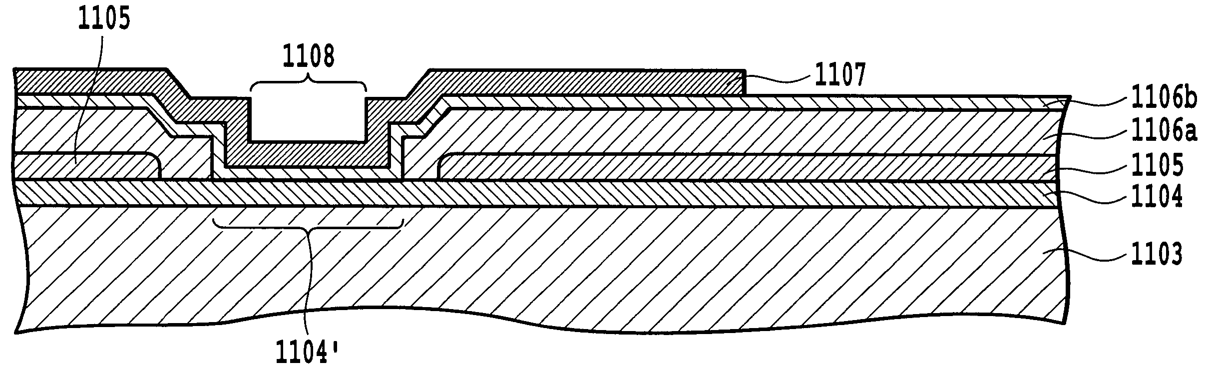
[0041]FIG. 4 and FIG. 5 are a schematic plan view of the vicinity of a heater of an ink jet head circuit board according to a first embodiment of the present invention and a cross-sectional view taken along the V-V line of it, respectively. Here, portions functioning as similar to the respective portions in FIG. 1 to FIG. 3 are designated with the same reference numerals.

[0042]This embodiment basically applies a configuration to form two l...


PUM


Abstract

In an ink jet head circuit board including a heater for generating thermal energy used for ejecting ink in response to application of electricity, a drop in thermal energy efficiency is prevented while reducing an area of the heater to achieve higher-resolution and higher-image-quality printing, and damages on the heater attributable to a manufacturing process are avoided. To achieve this, a resistor layer is disposed on an electrode wire layer; and two protective layers are disposed thereon. Then the upper protective layer is removed in a site above the heater. Accordingly, it is possible to dispose the protective layers without causing a decrease in an effective bubble generating region, and to improve thermal energy efficiency by reducing the effective thickness of the protective layer above the heater. Moreover, the resistor layer is covered with the first protective layer and is thereby prevented from adverse effects in the manufacturing process such as etching processes.

Description

BACKGROUND OF THE INVENTION[0001]1. Field of the Invention[0002]The present invention relates to a circuit board for an ink jet head that ejects ink for printing, a method of manufacturing the circuit board, and an ink jet head using the circuit board.[0003]2. Description of the Related Art[0004]An ink jet printing system has a characteristic that it is possible to print a high-definition image at a high speed by ejecting a very small amount of ink out of a nozzle in the form of droplets, for example. There are a variety of ejection methods available for the ink jet printing head (hereinafter referred simply as a printing head when appropriate) to realize the ink jet printing system. Among them, ink jet heads using methods of ejecting ink by use of thermal energy have been disclosed in U.S. Pat. Nos. 4,723,129, 4,740,796, and the like. A head according to the foregoing methods includes an ink jet head circuit board provided with a plurality of heaters for heating ink and generating ...

Claims


Application Information

Patent Timeline
Patent Type & Authority Patents(United States)
IPC IPC(8): B41J2/05
CPCB41J2/14129B41J2/1603B41J2/1628B41J2/1629B41J2/1642B41J2/1645B41J2/1646B41J2/1631H05K1/167B41J2202/03
Inventor SAITOSAKAI, TOSHIYASUOZAKI, TERUOYOKOYAMA, SAKAIONO, KENJIIBE, SATOSHISHIBATA, KAZUAKI
Owner CANON KK
Learn More