Actuator system

a technology of actuators and actuators, applied in the field of actuator systems, can solve the problems of not being able to accurately control, not being able to use electromagnetic driving schemes, and not being able to achieve high-speed operation, and reducing the size of piezoelectric elements 117, achieving precise system operation, and reducing the amount of movement for one cycle

Inactive Publication Date: 2009-07-28
HITACHI LTD
View PDF3 Cites 6 Cited by
  • Summary
  • Abstract
  • Description
  • Claims
  • Application Information

AI Technical Summary

Benefits of technology

[0011]And, in the piezoelectric driving-electrostatic adsorption type, in which a rapid deformation of a piezoelectric element and friction force of the contact surface are used, an amount of deformation of the piezoelectric element for one time corresponds to one step of movement of a moving element. Deformation of the piezoelectric element is caused due to the ratio of crystalline distortion. In principle, as the dimension of the piezoelectric element is decreased, an amount of crystalline distortion is also decreased. If the probe memory is downsized, the piezoelectric element is also downsized, and as a result, a multi-axial-movement-type actuator system having a recording medium with a small amount of movement for one step mounted thereon can be achieved. Accordingly, for an information storage device for an information terminal, mainly a mobile device, downsizing, high density (large capacity), and low voltage are required, and therefore the piezoelectric driving-electrostatic adsorption type is advantageous.
[0019]First, in STEP 1 which is a start of the operation of the actuator 101, LOW is applied to the carrier electrode 115, whilst HIGH is applied to the driving electrode 118, thereby providing a potential difference between the carrier electrode 115 and the driving electrode 118 to adsorb with electrostatic force.
[0026]And, in principle, an amount of movement of the carrier stage 111 for one cycle corresponds to the amount of electrostriction of the piezoelectric element 117. And therefore, as the dimension of the piezoelectric element 117 is decreased, the amount of movement for one cycle is decreased. That is, the actuator 101 studied by the present inventors employs an actuator control scheme achieving both microfabrication and precise operation of the system.
[0031]Another object of the present invention is to provide a technology capable of operating an actuator using a piezoelectric element at high speed.
[0036]According to the present invention, the actuator using the piezoelectric element can be stably operated. And, the actuator using the piezoelectric element can be operated at high speed.

Problems solved by technology

And therefore, the electromagnetic driving scheme, such as the one disclosed in the Non-Patent Document 1, for example, is not suitable in principle to accurately control the amount of movement of the media-mounting stage per one step, and is not suitable for a probe memory that requires operation of a pitch of 25 nm per one step.
For this reason, the electromagnetic driving scheme is not suitable for high-speed operation.

Method used


Image

  • Actuator system
  • Actuator system
  • Actuator system

Examples


first embodiment

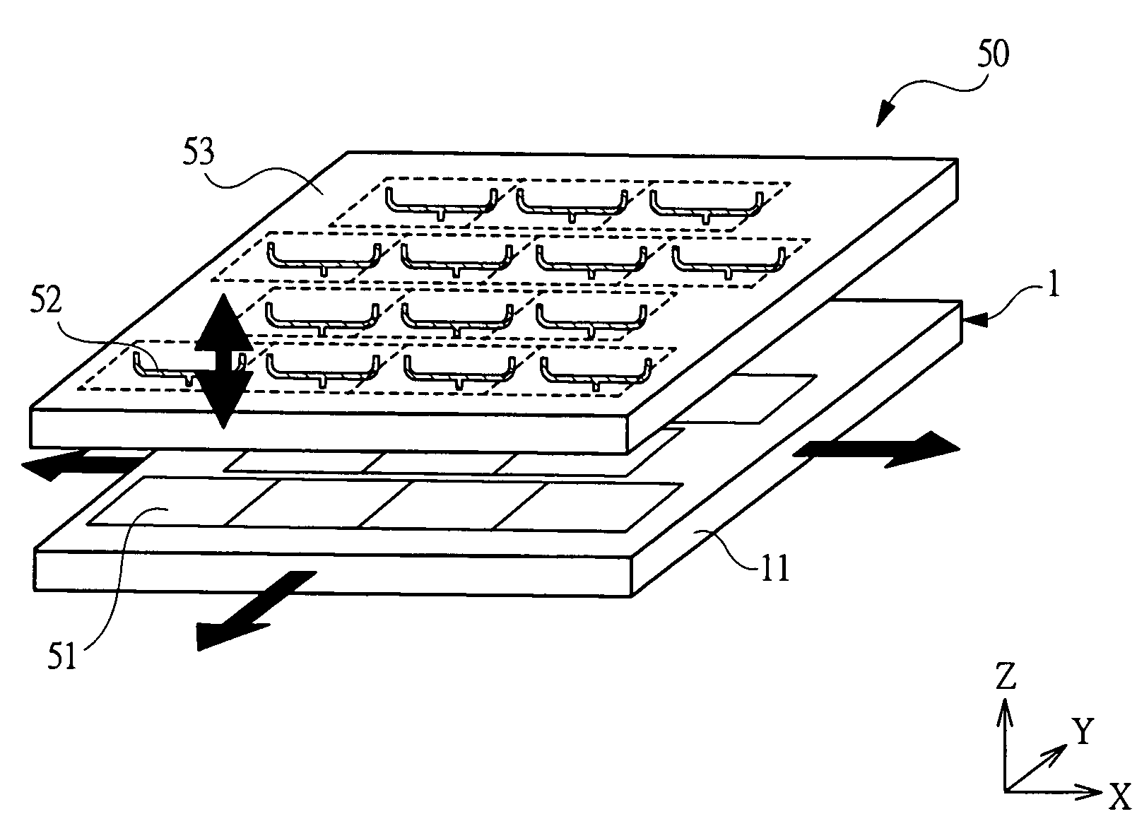
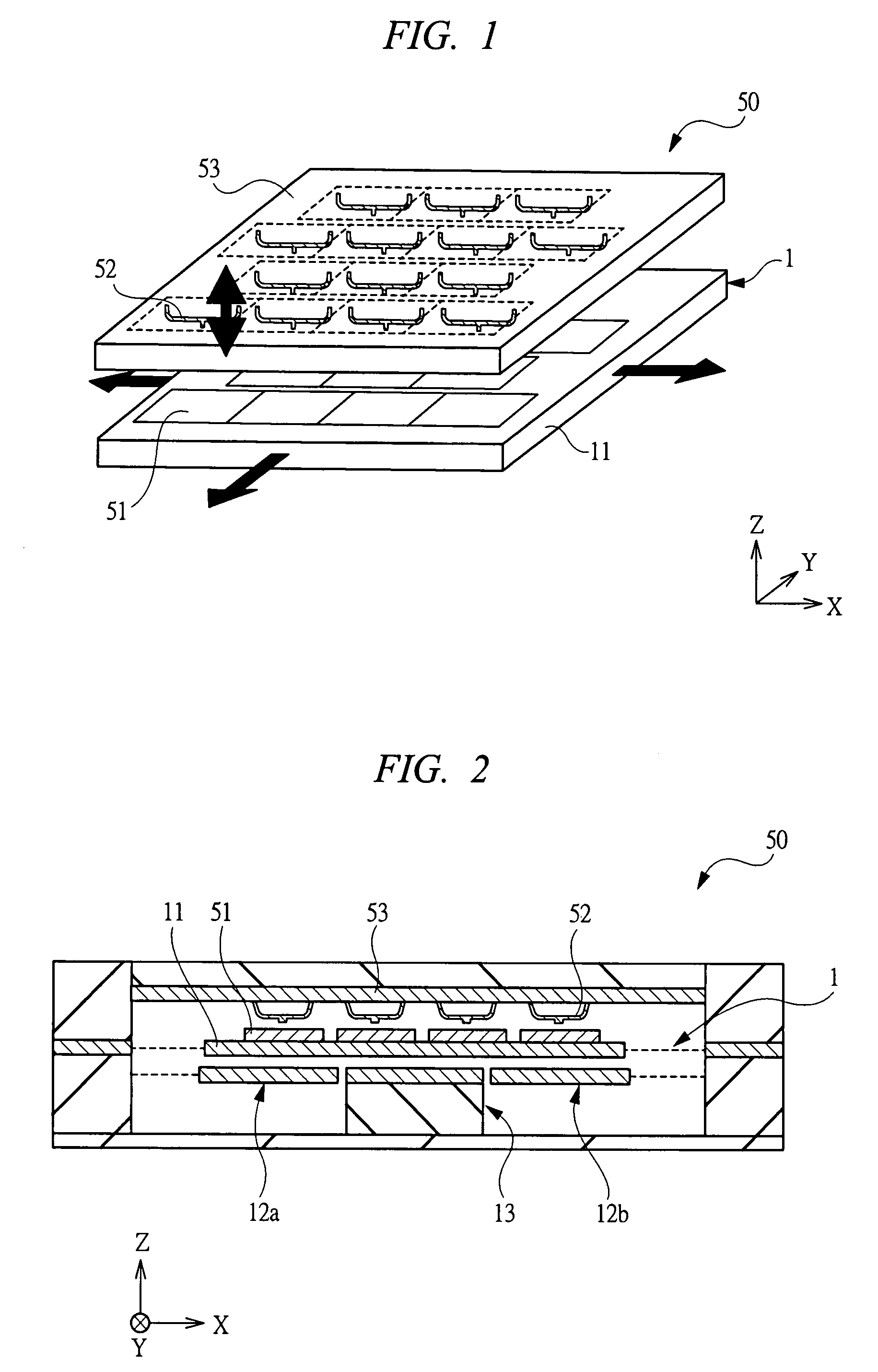
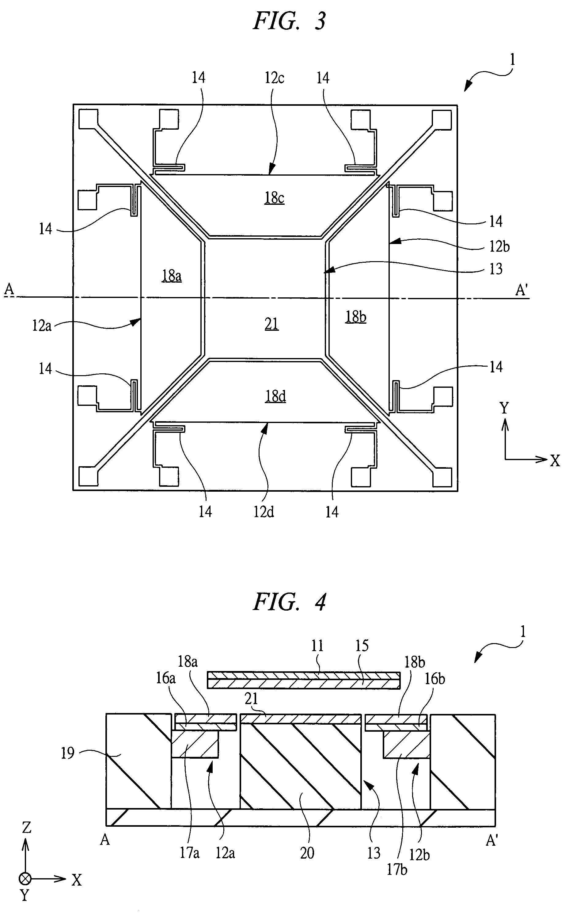
[0074]First, a configuration of a probe memory including an actuator system of piezoelectric driving-electrostatic adsorption type (hereinafter referred to as an actuator) according to a first embodiment of the present invention is described using FIGS. 1 and 2. FIG. 1 is a perspective diagram of a probe memory 50 including an actuator 1 according to the first embodiment. FIG. 2 is a cross-sectional diagram of the probe memory 50 of FIG. 1 sectioned at a center position. Note that, in FIG. 2, for ease of description, a carrier stage 11 is shown as being separated from driving units 12a, 12b and a holding unit 13. In practice, however, the carrier stage 11 is provided so as to make contact with the driving units 12a, 12b and the holding unit 13.

[0075]The probe memory 50 is provided with a plurality of probes 52 including one or more small probes (probe chips) for performing information writing to or information reading from a recording medium 51, a first substrate 53 having a signal ...

second embodiment

[0118]In the first embodiment, the case has been described in which the actuator system of the piezoelectric driving-electrostatic adsorption type includes the holding unit provided with the holding electrode in the mechanism of driving the carrier stage having the recording medium mounted thereon in the X-Y axes directions. However, in a second embodiment, a case in which the holding unit is not included is described.

[0119]A configuration of an actuator system of the piezoelectric driving-electrostatic adsorption type (hereinafter referred to as an actuator) according to the second embodiment is described using FIGS. 13 and 14. FIG. 13 is a plan diagram of an actuator 2 according to the second embodiment. FIG. 14 is a cross-sectional diagram along a B-B′ line in FIG. 13. Note that, in FIG. 13, although a carrier stage 11 is omitted, the carrier stage 11 has a rectangular shape in a plan-view shape of X-Y plane, as shown in FIG. 1. And, in FIG. 14, for ease of description, the carri...

third embodiment

[0153]An actuator system of the piezoelectric driving-electrostatic adsorption type (hereinafter referred to as an actuator) according to a third embodiment of the present invention is described using FIGS. 17, 18A, and 18B. FIG. 17 is a cross-sectional diagram of a main part of an actuator according to the third embodiment. FIGS. 18A and 18B are timing charts of control signals of the actuator of FIG. 17. FIG. 18A shows control signals for a driving system, whilst FIG. 18B is shows a control signal for a carrying system. Note that, in FIG. 17 for ease of description, a carrier stage 11 is shown as being separated from driving units 12a, 12b and a holding unit 13. In practice, however, the carrier stage 11 is provided so as to make contact with the driving units 12a, 12b and the holding unit 13.

[0154]As shown in FIG. 17, the actuator 3 according to the third embodiment includes the carrier stage 11 composed of a substrate moving in biaxial directions (X-Y axes directions), the first...


PUM


Abstract

An actuator using a piezoelectric element is stably operated at high speed. The actuator includes driving units provided to face a carrier stage and moving the carrier stage in an X-axis direction, piezoelectric elements provided to the driving units respectively and expanding and contracting in the X-axis direction, a carrier electrode provided on a surface of the carrier stage on a driving-unit side, and driving electrodes provided on surfaces of the driving units on a carrier stage side and electrostatically adsorbing the carrier electrode. Signals not synchronized with each other are applied to the piezoelectric elements.

Description

CROSS-REFERENCE TO RELATED APPLICATION[0001]The present application claims priority from Japanese Patent Application No. JP 2006-277559 filed on Oct. 11, 2006, the content of which is hereby incorporated by reference into this application.TECHNICAL FIELD OF THE INVENTION[0002]The present invention relates to an actuator system and, in particular, to a technology effective when applied to an actuator system using a piezoelectric element.BACKGROUND OF THE INVENTION[0003]A probe memory technology using a principle of a Scanning Probe Microscope (SPM) is a promising technology for an information recording device dramatically increasing recording density. An information storage device using such a probe memory technology (hereinafter referred to as a probe memory) includes a recording medium, an actuator system driving the recording medium mounted over a stage (substrate) in X-axis and Y-axis directions (biaxial directions), a probe including one or more microprobes (hereinafter referred...

Claims


Application Information

Patent Timeline
Patent Type & Authority Patents(United States)
IPC IPC(8): H01L41/08
CPCH02N2/028H02N2/021G11B9/1436B82Y10/00
Inventor YAMANAKA, KIYOKOGOTO, YASUSHIHASEBE, TAKEHIKO
Owner HITACHI LTD
Why Eureka
Try Eureka