Semiconductor acceleration sensor device and method for manufacturing the same

a sensor device and semiconductor technology, applied in the direction of acceleration measurement using interia force, instruments, television systems, etc., can solve the problem of easy displacement by external acceleration, and achieve the effect of maintaining long-term reliability and excellent mass production

Inactive Publication Date: 2009-08-04
LAPIS SEMICON CO LTD
View PDF18 Cites 21 Cited by
  • Summary
  • Abstract
  • Description
  • Claims
  • Application Information

AI Technical Summary

Benefits of technology

[0017]One object of the present invention is to provide a semiconductor acceleration sensor device which is low-cost and excellent for mass production while maintaining long-term reliability, and also to provide a method for manufacturing such a semiconductor acceleration sensor device. The semiconductor acceleration sensor device is provided through giving low-cost resin packaging to an MEMS chip by filling the inside of the MEMS chip with a gel material and coating the MEMS chip with the gel material.
[0019]Although the weight part of the acceleration sensor chip is coated with the elastic first resin part, it is easily displaced by an external acceleration. Therefore, an acceleration can be detected with accuracy. Furthermore, long-term reliability equal to those of regular resin packages is ensured because those portions of the acceleration sensor device which are not used for acceleration sensing are sealed with the second resin part. Thus, compared to conventional devices, a device of lower-cost and higher mass productivity can be expected.
[0021]According to this method, a semiconductor acceleration device which is excellent in long-term reliability can be mass-produced at a low cost through relatively simple process.
[0025]According to this manufacturing method, a semiconductor acceleration sensor device excellent in long-term reliability can be mass-produced at a lower cost through simpler manufacturing process.

Problems solved by technology

Although the weight part of the acceleration sensor chip is coated with the elastic first resin part, it is easily displaced by an external acceleration.

Method used


Image

  • Semiconductor acceleration sensor device and method for manufacturing the same
  • Semiconductor acceleration sensor device and method for manufacturing the same
  • Semiconductor acceleration sensor device and method for manufacturing the same

Examples


first embodiment

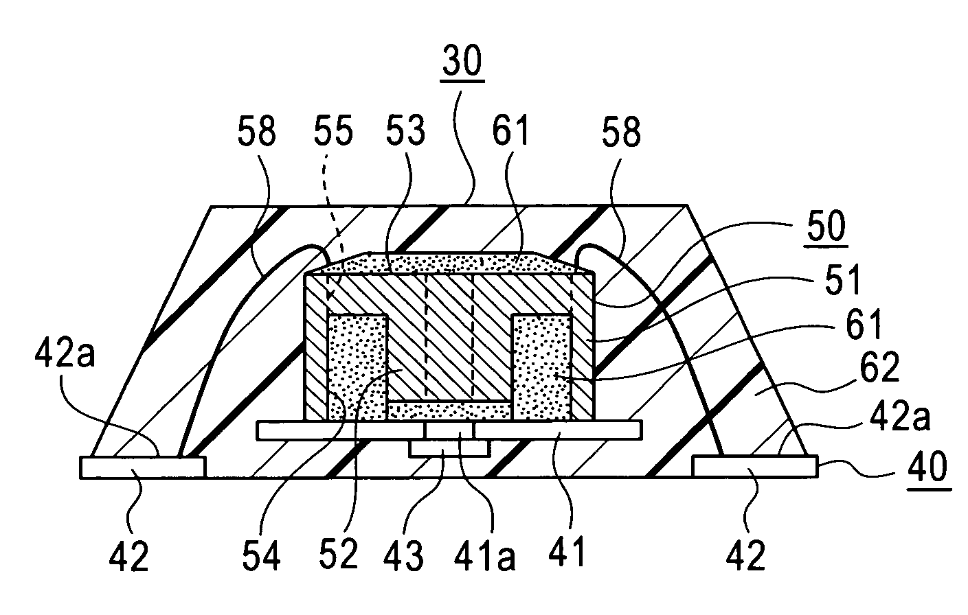
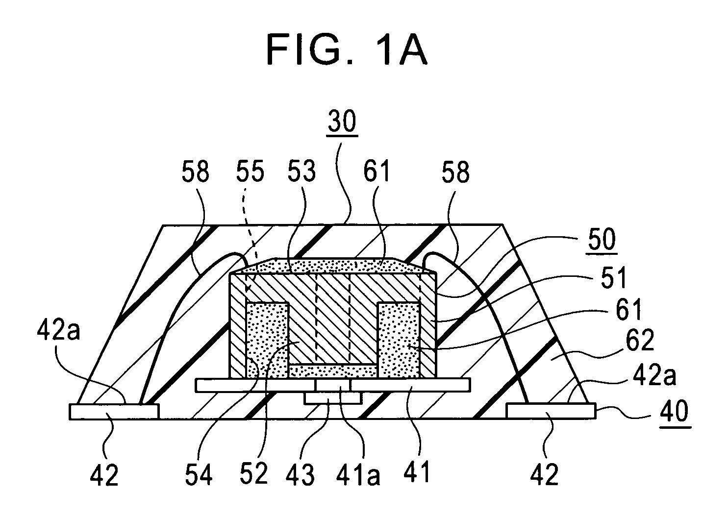
[0036]Referring to FIGS. 1A to 1F, a QFN package type semiconductor acceleration sensor device according to a first embodiment of the present invention will be described.

[0037]The semiconductor acceleration sensor device 30 is mounted on a lead frame 40. The lead frame 40 has a die pad 41 which is a rectangular supporting plate. In a first area of the die pad 41 which occupies the central portion of the die pad 41 is formed a first through hole 41a. Four conductive parts (for example, post sections) 42a of a plurality of leads 42 are provided around the die pad 41. On the lower surface of the die pad 41 is fixed a lid part 43 to close the through hole 41a. In a second area of the die pad 41, which surrounds the first area which occupies the central portion of the upper surface of the die pad 41 is fixed an acceleration sensor chip 50 which detects external acceleration.

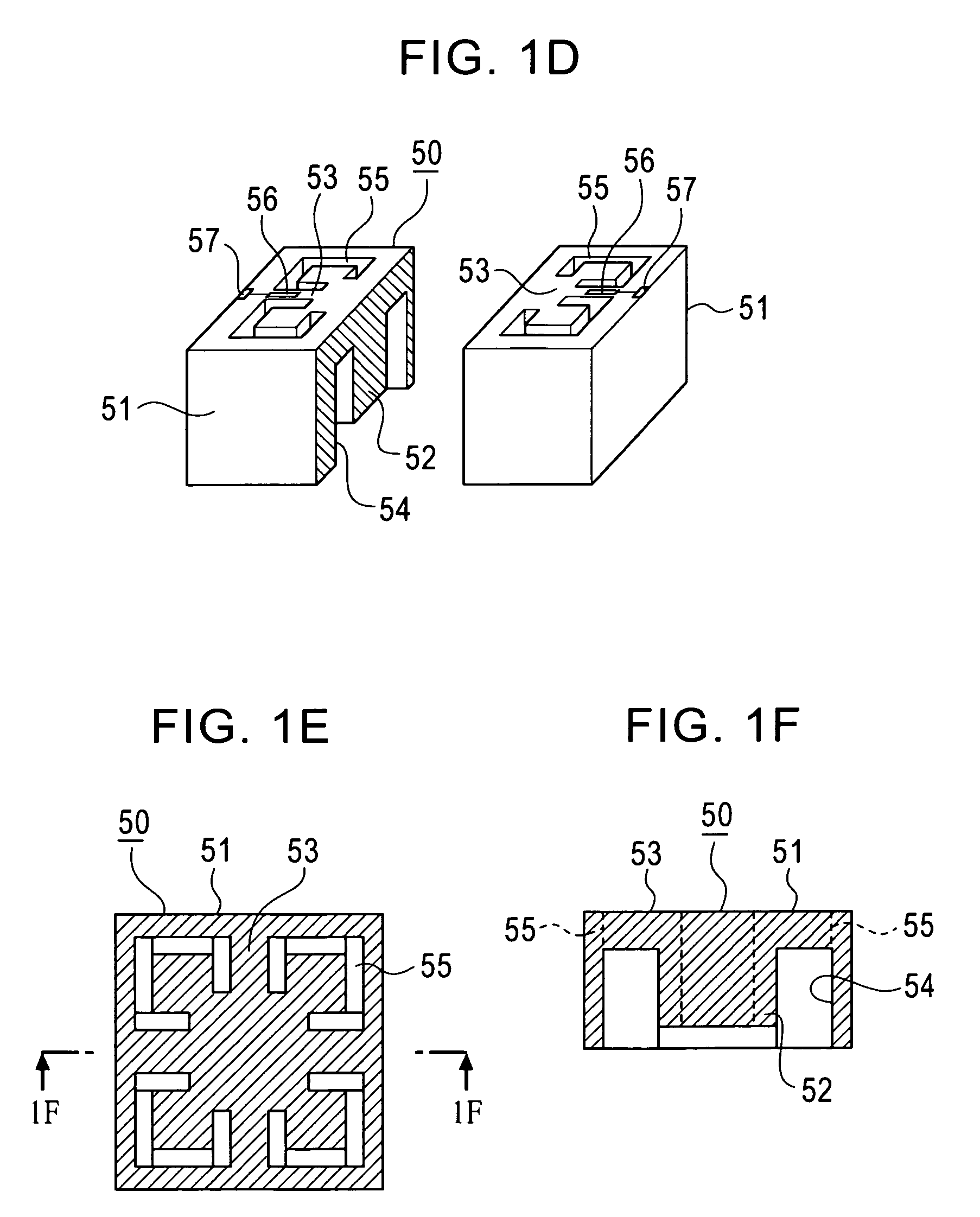
[0038]The acceleration sensor chip 50 has a pedestal part (for example, a silicon chip or a semiconductor chip) 51....

second embodiment

[0047]FIGS. 2A to 2D show a series of manufacturing steps to fabricate the semiconductor acceleration sensor device 30 shown in FIG. 1.

[0048]The semiconductor acceleration sensor device 30 is manufactured, for example through the following steps (1) to (4).

[0049](1) Step of FIG. 2A

[0050]The acceleration sensor chip 50 of FIG. 1 is prepared in advance. The acceleration sensor chip 50 is positioned on the die pad 41 of the lead frame 40. The die pad 41 is coupled to a plurality of other die pads 41 via the leads 42. The lower surface of the acceleration sensor chip 50 is die-bonded (fixed) on the upper surface of the die pad 41 with an adhesive or the like. When the die pad 41 does not function sufficiently as a stopper due to shortness of the weight part 52, a spacer having a through hole may be disposed beforehand on the die pad 41 so that the spacer serves as the stopper. After the electrode pads 57 on the upper surface of the acceleration sensor chip 50 are bonded (connected) to t...

third embodiment

[0062]FIGS. 3A to 3D show another series of manufacturing steps to fabricate the semiconductor acceleration sensor device 30 shown in FIG. 1. This method is similar to that of the second embodiment. The semiconductor acceleration sensor device 30 is manufactured, for example, through the following steps (1) to (4).

[0063](1) Step of FIG. 3A

[0064]In the same manner as shown in FIG. 2A, the acceleration sensor chip 50 is die-bonded on the die pad 41 of the lead frame 40. After the electrode pads 57 of the acceleration sensor chip 50 are bonded to the post sections 42a of the lead frame 40 by the wires 58, the lead frame 40 is turned upside down as shown in FIG. 3A.

[0065](2) Step of FIG. 3B

[0066]The needle 63 for resin injection is positioned over the through hole 41a provided in the center of the die pad 41. Then, from the needle 63 the viscous liquid resin (for example, such as a thermosetting silicon resin) 61a is injected into the through hole 41a by only enough amount to coat the u...


PUM


Abstract

Although a weight part of an acceleration sensor chip fixed on a die pad is coated with a gelatinous resin part of low elasticity, the weight part is easily displaced by an external acceleration. Thus, an acceleration can be detected with accuracy. Furthermore, long-term reliability equal to those of regular resin packages is ensured because those portions of an acceleration sensor device which are not used for acceleration sensing are sealed with a resin part.

Description

BACKGROUND OF THE INVENTION[0001]1. Field of the Invention[0002]This invention relates to a semiconductor acceleration sensor device utilizing a resin sealed package and a method for manufacturing the device. More particularly, this invention relates to the device utilizing an MEMS (Micro Electro Mechanical Systems) or an MCP (Multi Chip Package). The MCP is a package on which an MEMS and a semiconductor circuit chip are mounted together.[0003]2. Description of the Related Art[0004]In recent years, with reduced sizes and thicknesses of electronic devices, attention is focused on an MEMS technology, which enables fabrication of sensors or electromechanical parts or the like in a micrometer size.[0005]FIGS. 8A to 8C of attached drawings show cross-sectional views of examples of the constitution of semiconductor acceleration sensor devices utilizing a conventional MEMS package. FIG. 8A illustrates a single-chip type device, FIG. 8B a multi-chip type (a stacked type) device, and FIG. 8C...

Claims


Application Information

Patent Timeline
Patent Type & Authority Patents(United States)
IPC IPC(8): G01P1/02G01P15/12G01P15/08B81B7/02H01L21/56H01L23/28
CPCG01P1/023G01P15/123G01P15/18H01L2224/48091H01L2224/48137H01L2224/48247H01L2924/1461H01L2924/10253H01L2924/00014H01L2924/00H01L24/97G01P2015/0842A47J37/0676A47J37/0786A23L5/30
Inventor SHIZUNO, YOSHINORI
Owner LAPIS SEMICON CO LTD
Why Eureka
Try Eureka